Defect detecting device, image sensor device, and image sensor module
A defect detection and defect technology, applied in image enhancement, image analysis, image data processing, etc., can solve the problems of larger circuit structure and longer time, and achieve the effect of compact circuit structure
- Summary
- Abstract
- Description
- Claims
- Application Information
AI Technical Summary
Problems solved by technology
Method used
Image

Examples
Embodiment Construction
[0081] (1. Basic structure of the device)
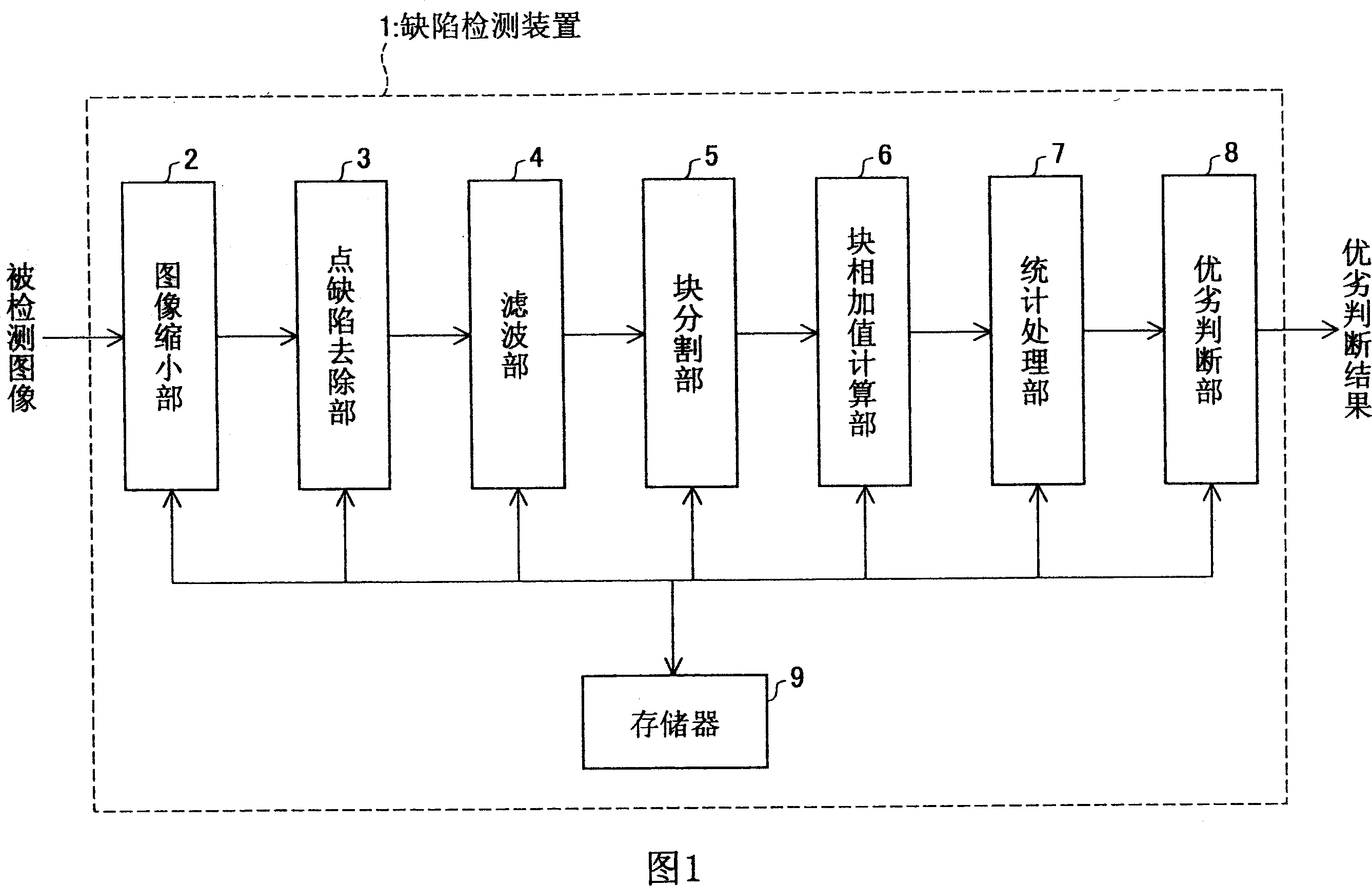
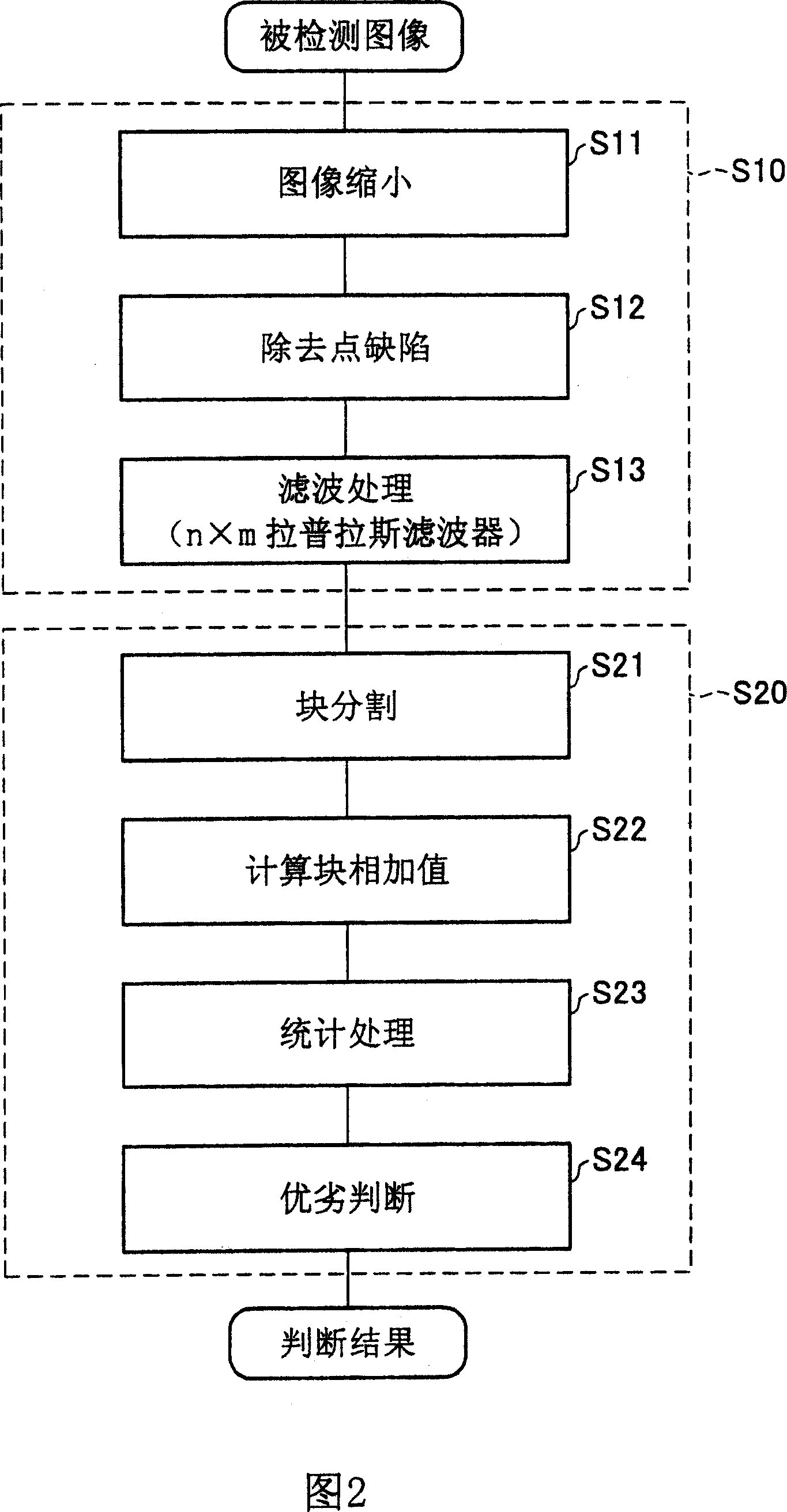
[0082] One embodiment of the defect detection device of the present invention will be described using FIG. 1 . As shown in FIG. 1 , the defect detection device 1 of the present embodiment includes: an image reduction unit (image reduction device) 2, a point defect removal unit (point defect removal device) 3, a filtering unit (filtering device) 4, and a block division unit (block division device) 5, block addition value calculation unit (block addition value calculation unit) 6, statistical processing unit (defect area presence or absence judgment unit) 7, good or bad judgment unit (defect area presence or absence judgment unit) 8 , memory 9.
[0083] The image reduction unit 2 performs a process of reducing the vertical size and the horizontal size of the detected image to reduce the detected image. Thereby, the amount of data of the detected image can be reduced, and the speckle defect and lump defect existing in the detected ima...
PUM
 Abstract
Description
Claims
Application Information
 - R&D
- Intellectual Property
- Life Sciences
- Materials
- Tech Scout
- Unparalleled Data Quality
- Higher Quality Content
- 60% Fewer Hallucinations
Browse by: Latest US Patents, China's latest patents, Technical Efficacy Thesaurus, Application Domain, Technology Topic, Popular Technical Reports.
© 2025 PatSnap. All rights reserved.Legal|Privacy policy|Modern Slavery Act Transparency Statement|Sitemap|About US| Contact US: help@patsnap.com