Implementing decreased scan data interdependence for compressed patterns in on product multiple input signature register (OPMISR) through scan skewing

a technology of multiple input signature register and scan data, applied in the field of data processing, can solve the problems of large amount of data for analysis, high cost, and easy introduction of defects in circuits, and achieve the effect of reducing noise or power

Inactive Publication Date: 2019-07-23
IBM CORP
View PDF23 Cites 0 Cited by
  • Summary
  • Abstract
  • Description
  • Claims
  • Application Information

AI Technical Summary

Benefits of technology

[0008]Principal aspects of the present invention are to provide a method and circuit for implementing enhanced scan data testing with decreased scan data interdependence for compressed patterns in on product multiple input signature register (OPMISR) testing through scan skewing, and a design structure on which the subject circuit resides. Other important aspects of the present invention are to provide such method, circuit and design structure substantially without negative effects and that overcome many of the disadvantages of prior art arrangements.
[0011]In accordance with features of the invention, the chiplet selected circuit allows better fitting of care bits for test compaction. For example, when two test pattern care bit locations conflict, rather than requiring a full new test, a small shift in loading one chiplet can allow the tests to be combined at a much smaller cost of only a few scan clocks.
[0012]In accordance with features of the invention, the chiplet selected circuit effectively and efficiently enables generating and combining test patterns.
[0016]In accordance with features of the invention, the chiplet selected circuit enables a balance point to be reached for all patterns, and the patterns can be filled. Filling is either with random data or based on another criteria, like minimizing switching for the entire pattern to reduce noise or power.

Problems solved by technology

Circuits often are prone to defects introduced during a manufacturing process.
Typically the tests take a great amount of time, produce large amounts of data for analysis, and require large amounts of resources for that analysis.
Plus, test tend to require a lot of time since the entire chip is scanned in and out in each test iteration.
This can simply make some logic untestable or at least reduce fault coverage per cycle.
This is because as each test targets a specific section of logic; feeding that same test data to other sections may not do as good a job of detecting faults there.
While this significantly reduces data volume it could limit test coverage where common data initialization conflicts with a unique need for testing a structure.

Method used


Image

  • Implementing decreased scan data interdependence for compressed patterns in on product multiple input signature register (OPMISR) through scan skewing
  • Implementing decreased scan data interdependence for compressed patterns in on product multiple input signature register (OPMISR) through scan skewing
  • Implementing decreased scan data interdependence for compressed patterns in on product multiple input signature register (OPMISR) through scan skewing

Examples


Embodiment Construction

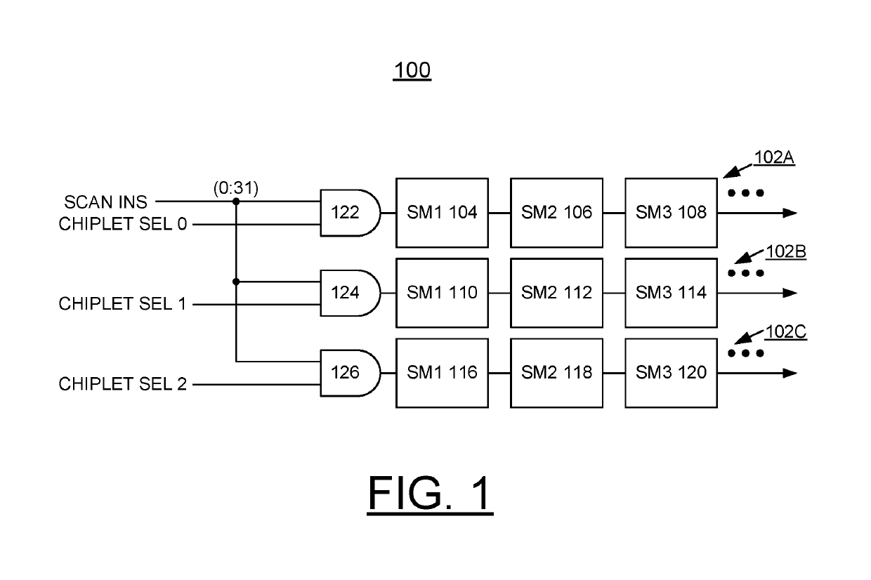
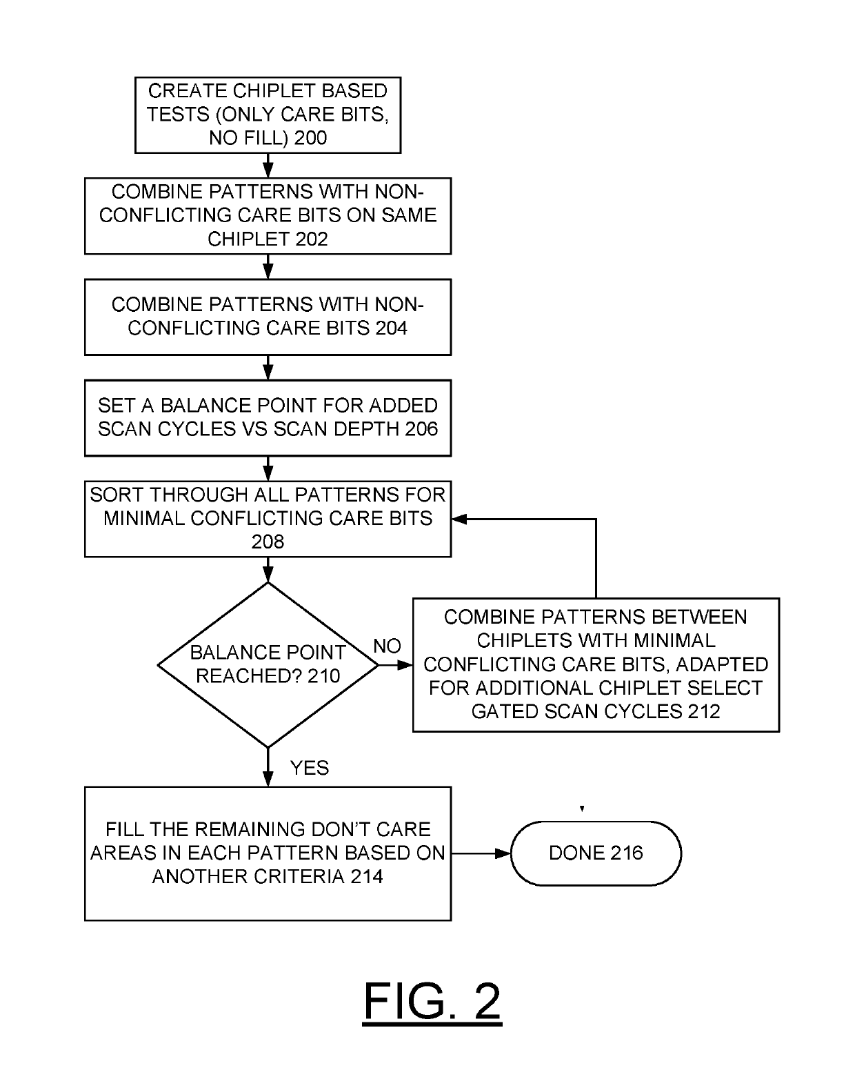
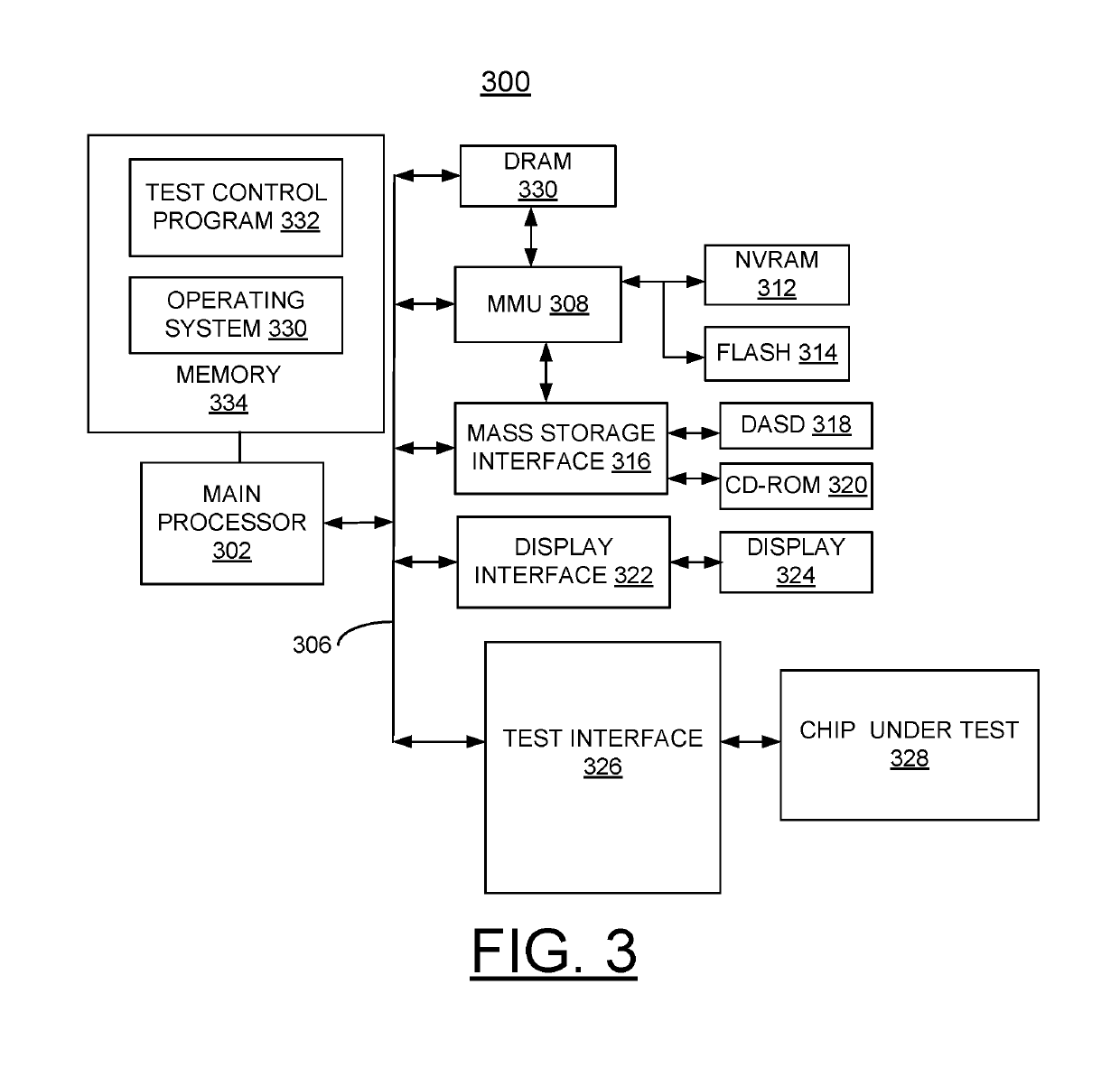
[0023]In the following detailed description of embodiments of the invention, reference is made to the accompanying drawings, which illustrate example embodiments by which the invention may be practiced. It is to be understood that other embodiments may be utilized and structural changes may be made without departing from the scope of the invention.

[0024]The terminology used herein is for the purpose of describing particular embodiments only and is not intended to be limiting of the invention. As used herein, the singular forms “a”, “an” and “the” are intended to include the plural forms as well, unless the context clearly indicates otherwise. It will be further understood that the terms “comprises” and / or “comprising,” when used in this specification, specify the presence of stated features, integers, steps, operations, elements, and / or components, but do not preclude the presence or addition of one or more other features, integers, steps, operations, elements, components, and / or gr...


PUM


Abstract

A method and circuit for implementing enhanced scan data testing with decreased scan data interdependence for compressed patterns in on product multiple input signature register (OPMISR) testing through scan skewing, and a design structure on which the subject circuit resides are provided. The circuit is divided into multiple chiplets. Each chiplet includes a stump mux structure including multiple stump muxes connected in series, and a respective chiplet select is provided on shared scan inputs to respective chiplets. The chiplet select gates scan clocks, and when a chiplet is not selected the chiplet retains its data. The chiplet select enables test data to be skewed as scan data enters each chiplet.

Description

FIELD OF THE INVENTION[0001]The present invention relates generally to the data processing field, and more particularly, relates to a method and circuit for implementing enhanced scan testing with decreased scan data interdependence for compressed patterns in on product multiple input signature register (OPMISR) testing through scan skewing, and a design structure on which the subject circuit resides.DESCRIPTION OF THE RELATED ART[0002]Circuits often are prone to defects introduced during a manufacturing process. To test for defects, a scan input may be applied to scan channels, and the result of the scan input that is applied to the scan channels may be analyzed. The test may include large numbers and variations of scan inputs being applied to scan channels of the circuit. Typically the tests take a great amount of time, produce large amounts of data for analysis, and require large amounts of resources for that analysis.[0003]As Application Specific Integrated Circuit (ASIC) and Pr...

Claims


Application Information

Patent Timeline
Patent Type & Authority Patents(United States)
IPC IPC(8): G01R31/3177G01R31/317G01R31/327
CPCG01R31/31725G01R31/3177G01R31/318547G01R31/318563
Inventor DOUSKEY, STEVEN M.HAMILTON, MICHAEL J.KAUFER, AMANDA R.SENUM, PHILLIP A.
Owner IBM CORP
Why Eureka
Try Eureka