Voltage modulated driver circuits for electro-optic displays

a driver circuit and electro-optic technology, applied in the field of electro-optic displays, can solve the problems of inadequate service life of these displays, unable to meet the needs of users, and gas-based electrophoretic media are susceptible to the same types of problems, so as to achieve faster design time, reduce complexity, and reduce the cost of implementation

Active Publication Date: 2007-08-30
E INK CORPORATION
View PDF3 Cites 140 Cited by
  • Summary
  • Abstract
  • Description
  • Claims
  • Application Information

AI Technical Summary

Benefits of technology

[0039] The first aspect of the present invention can provide, for example, lower cost of implementation for column driver circuits, faster design time and lower complexity, to decrease time-to-market and development risk. Smaller die size of integrated circuits (ICs) can decrease cost and increase yield. Smaller dice on a polycrystalline silicon panel can permit, for example, fabrication of more panels on a glass substrate or increase the fraction of panel footprint available for pixels.
[0040] In one embodiment of the first aspect of the invention, the number of transistors required to implement a power rail switching scheme is less than the number of transistors required to implement a conventional R-DAC system. The number of transistors can be further reduced when the number of voltage levels provided by the driver circuit is relatively low (for example, approximately 16 or fewer.) When the transistors are operated only in saturation mode, and no sensitive analog nodes exist in the circuit, a driver design can produce more accurate output levels, and can be less complex and easier to design, analyze, fabricate, and test.

Problems solved by technology

Nevertheless, problems with the long-term image quality of these displays have prevented their widespread usage.
For example, particles that make up electrophoretic displays tend to settle, resulting in inadequate service-life for these displays.
Such gas-based electrophoretic media appear to be susceptible to the same types of problems due to particle settling as liquid-based electrophoretic media, when the media are used in an orientation which permits such settling, for example in a sign where the medium is disposed in a vertical plane.
Indeed, particle settling appears to be a more serious problem in gas-based electrophoretic media than in liquid-based ones, since the lower viscosity of gaseous suspending fluids as compared with liquid ones allows more rapid settling of the electrophoretic particles.
Although a DAC-based architecture has many benefits, it typically requires a large number of transistors for implementation.
This can lead to two problems: 1) the implementation of the circuit can be complex with care required to insure proper functionality and accuracy; and 2) a large area of active circuit can be required, which can lead to higher cost (especially at higher voltages).
The cost of a large number of DACs in a high-resolution display may increase the manufacturing cost of a display.
Specialized processes may reduce the number of vendors available with a suitable manufacturing capability and may increase final cost as well as the complexity and cost of designing the architecture.
Although such slide show waveforms can produce accurate gray levels in the final image, they have the disadvantage that if all the pixels of the display are driven simultaneously to white and then to black, the user sees at least one “flash” between the initial and final images on the display.
Most users find such flashes distracting and annoying.
Another problem in updating bistable displays is that, in practice, because it normally necessary to use drivers with only a limited number of voltage levels, the greater the number of gray levels which have to be written, the greater the update time.
However, such a “double drive scheme” approach can give rise to additional problems.
As already indicated, it is normally necessary to drive bistable electro-optic displays using drivers capable of providing only a limited number of voltage levels, because drivers capable of applying large numbers of voltage levels are considerably more expensive.
Since only a limited number of driving voltages are available, the impulses which can be applied to the pixel (these impulses being proportional to the areas of the aforementioned rectangles) are quantized, and it may be difficult to combine such quantized impulses to reproduce accurately the impulse needed for a particular gray level transition, and there may be some inaccuracy in the final gray level resulting from the transition.
Such inaccuracy in final gray level can give rise to a “areal ghosting” problem.
One cause of such ghost images is inaccuracy in gray levels during the rewriting of the display.

Method used


Image

  • Voltage modulated driver circuits for electro-optic displays
  • Voltage modulated driver circuits for electro-optic displays
  • Voltage modulated driver circuits for electro-optic displays

Examples


Embodiment Construction

[0074] As discussed above, this invention has three principal aspects, and these three principal aspects will primarily be described separately below. However, it should be understood that a single display may make use of more than one aspect of the present invention. For example, a display having an addressing architecture in accordance with the first aspect of the present invention may be used to carry out a drive method in accordance with the second or third aspect of the present invention.

[0075] Part A: Addressing Architecture

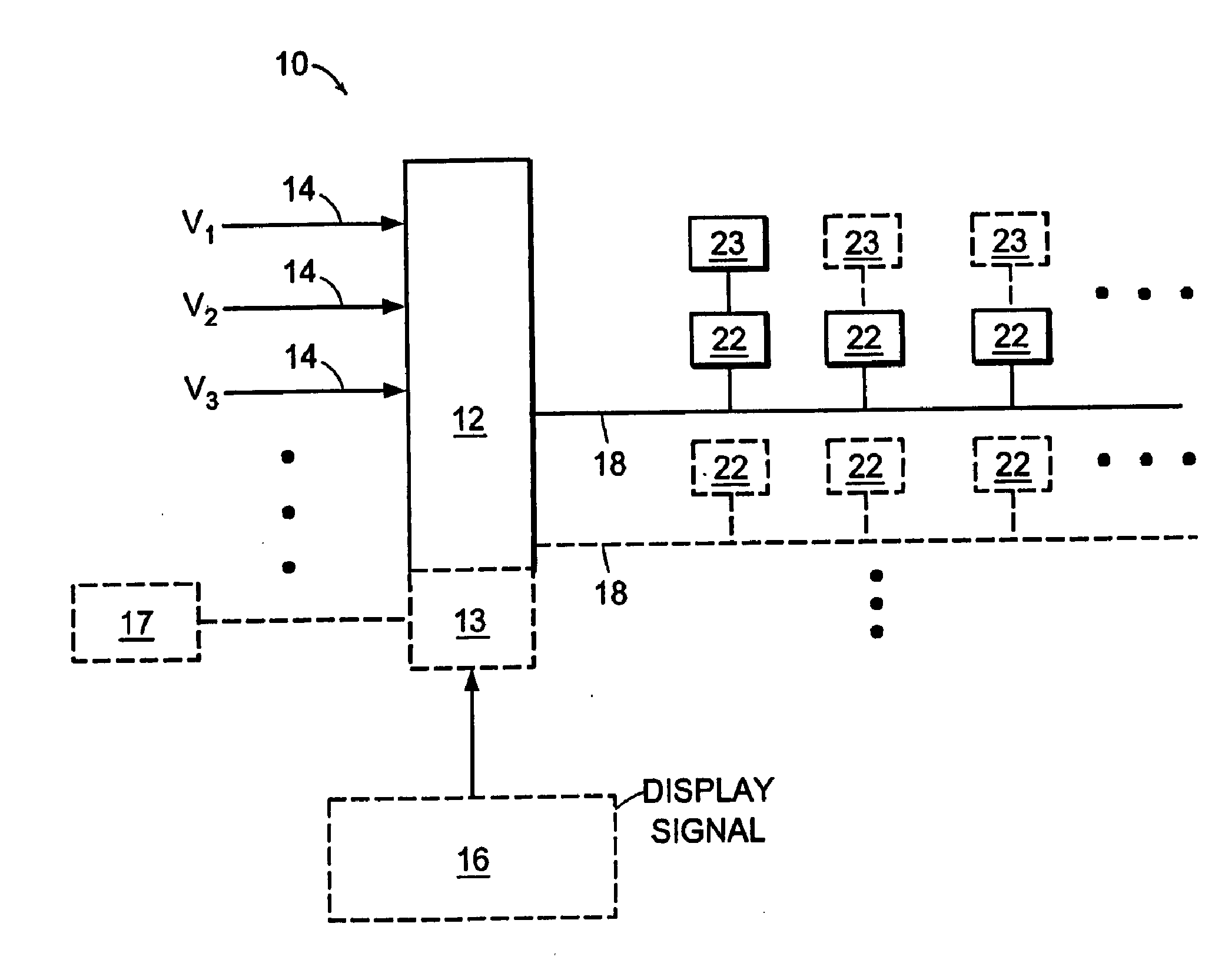
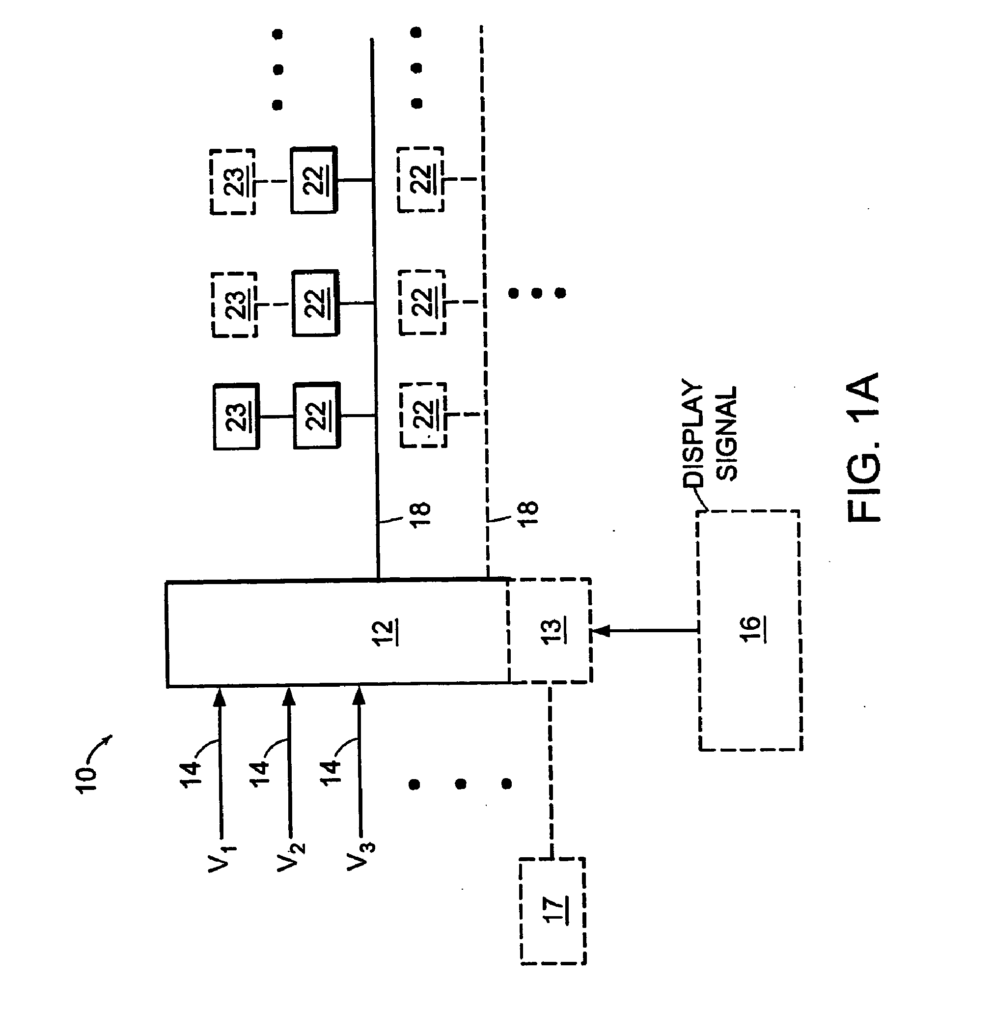
[0076]FIG. 1a is a schematic diagram of an embodiment of an addressing structure 10 of a display, according to principles of the invention. The display includes one or pairs of switch circuits 22 and pixel electrodes 23, which may be arranged in one or more columns and one or more rows. The addressing structure 10 includes a switch unit 12 that responds to a display signal, and one or more voltage sources 14 that are each associated with a voltage level V...


PUM


Abstract

A method and system for applying addressing voltages to pixels of a display involves receiving input data. The input data includes an indication of an addressing voltage impulse to be applied to a pixel via an electrode. One or more voltage sources are selected, to provide the addressing voltage impulse. The one or more voltage sources each have a pre-selected voltage, The selected one or more voltage sources are electrically connected to an electrode to apply the addressing voltage impulse to the pixel. The invention also provides a method of driving an electro-optic display which uses an intermediate image of reduced bit depth, and a method of driving an electro-optic display which uses a limited number of differing drive voltages, with higher voltage pulses being used before lower voltage pulses.

Description

CROSS-REFERENCE TO RELATED APPLICATIONS [0001] This application is a continuation-in-part of copending application Ser. No. 10 / 609,119, filed Jun. 27, 2003 (Publication No. 2004 / 0075634), which claims the benefit of U.S. Provisional Patent application Ser. No. 60 / 392,245, filed Jun. 28, 2002. [0002] This application is also a continuation-in-part of copending application Ser. No. 11 / 425,408, filed Jun. 21, 2006 (Publication No. 2006 / 0232531), which is itself a divisional of application Ser. No. 10 / 814,205, filed Mar. 31, 2004 (now U.S. Pat. No. 7,119,772, issued Oct. 10, 2006) which itself claims benefit of the following Provisional Applications: (a) Ser. No. 60 / 320,070, filed Mar. 31, 2003; (b) Ser. No. 60 / 320,207, filed May 5, 2003; (c) Ser. No. 60 / 481,669, filed Nov. 19, 2003; (d) Ser. No. 60 / 481,675, filed Nov. 20, 2003; and (e) Ser. No. 60 / 557,094, filed Mar. 26, 2004. [0003] This application is also a continuation-in-part of copending application Ser. No. 11 / 160,455, filed Jun...

Claims


Application Information

Patent Timeline
Patent Type & Authority Applications(United States)
IPC IPC(8): G06F3/038G09G5/10
CPCG09G3/344G09G2310/027G09G2310/0256G09G2300/08
Inventor AMUNDSON, KARL R.SJODIN, THEODORE A.SU, CHIA-CHENHARRINGTON, DEMETRIOUS MARKGATES, HOLLY G.
Owner E INK CORPORATION
Why Eureka
Try Eureka