Semiconductor device

a technology of semiconductors and devices, applied in the field of semiconductor devices, can solve problems such as the increase of the probability of errors occurring during the data transmission process

Active Publication Date: 2019-08-13
SK HYNIX INC
View PDF4 Cites 1 Cited by
  • Summary
  • Abstract
  • Description
  • Claims
  • Application Information

AI Technical Summary

Benefits of technology

[0008]According to the embodiments, by delaying data by a time for which an error correction operation is performed, advantages may be provided in that it is possible to secure the valid window of data in a write operation and a read operation.
[0009]Also, according to the embodiments, by delaying data by a time for which an error correction operation is performed, advantages may be provided in that it is possible to secure the margin of a strobe signal and data for performing a write operation and a read operation.

Problems solved by technology

In the case where an input / output speed of data is increased, the probability of an error to occur during a data transmission process increases.

Method used


Image

  • Semiconductor device
  • Semiconductor device
  • Semiconductor device

Examples


Embodiment Construction

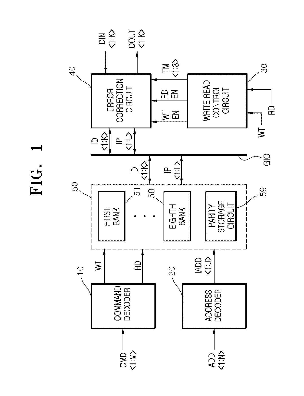
[0021]Hereinafter, a semiconductor device will be described below with reference to the accompanying drawings through various examples of embodiments.

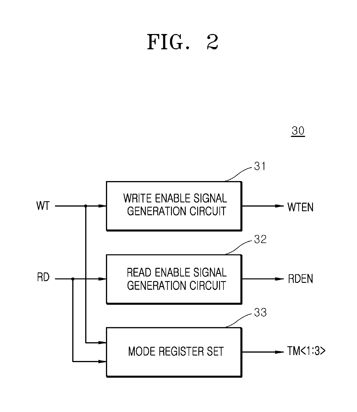
[0022]As shown in FIG. 1, a semiconductor device in accordance with an embodiment may include a command decoder 10, an address decoder 20, a write read control circuit 30, an error correction circuit 40, and a memory circuit 50.

[0023]The command decoder 10 may decode a command CMD1:M>, and generate a write command WT and a read command RD. The command CMD1:M> may be set as a signal inputted from a controller or test equipment which controls the semiconductor device. The command CMD1:M> may be transmitted through lines through which at least one of an address, a command and data is transmitted. The bit number M of the command CMD1:M> may be set as a natural number, and be set to various numbers of bits according to embodiments. The write command WT may be set as a command for entering a write operation. The read command RD may be set as...


PUM


Abstract

A semiconductor device includes a write read control circuit for outputting a write enable signal which is enabled in response to a write command, and a test mode signal; and an error correction circuit suitable for performing a calculation operation of determining an error information of input data in response to the write enable signal and then outputting an internal parity signal including the error information, and outputting internal data by delaying the input data in response to the write enable signal.

Description

CROSS-REFERENCE TO RELATED APPLICATION[0001]The present application claims priority under 35 U.S.C. § 119(a) to Korean Patent Application No. 10-2017-0004431 filed on Jan. 11, 2017 in the Korean Intellectual Property Office, which is incorporated herein by reference in its entirety.BACKGROUND1. Technical Field[0002]Embodiments of the present disclosure relate to a semiconductor device which performs an error correction operation for data.2. Related Art[0003]Recently, in order to increase the operating speed of a semiconductor device, DDR2 or DDR3 signaling is used, in which 4-bit or 8-bit data are inputted / outputted in each clock cycle. In the case where an input / output speed of data is increased, the probability of an error to occur during a data transmission process increases. Therefore, a separate device and method for ensuring the reliability of data transmission are additionally demanded.[0004]There is disclosed a method of generating, at each time of transmitting data, error c...

Claims


Application Information

Patent Timeline
Patent Type & Authority Patents(United States)
IPC IPC(8): G11C29/00G06F11/10G11C29/52G11C29/14G11C29/46G11C29/42G11C11/4096G11C11/4076
CPCG06F11/1068G06F11/1048G11C29/14G11C29/42G11C29/52G11C29/46G11C2207/229G11C11/4076G11C11/4096G11C13/0069G11C7/22G11C7/1078G11C7/1051G11C8/12
Inventor LEE, JAE INKIM, YONG MI
Owner SK HYNIX INC
Why Eureka
Try Eureka