Semiconductor memory device and method of operating the same

a memory device and semiconductor technology, applied in the field of semiconductor memory devices, can solve the problems of difficult to raise the breakdown voltage of a pass transistor

Active Publication Date: 2013-08-27
SK HYNIX INC
View PDF5 Cites 1 Cited by
  • Summary
  • Abstract
  • Description
  • Claims
  • Application Information

AI Technical Summary

Benefits of technology

[0006]This disclosure relates to a memory device and a method of operating the same, which are capable of narrowing a threshold voltage distribution of an erase state and securing the margin between threshold voltage distributions of a program state by supplying both a positive voltage and a negative voltage through a block switch.
[0007]Furthermore, this disclosure relates to a memory device and a method of operating the same, which are capable of lowering the breakdown voltages of the transistors of a block switch by setting the threshold voltages of the transistors to 0 V or lower in order to prevent a voltage drop phenomenon due to the block switch.

Problems solved by technology

However, raising the breakdown voltage of a pass transistor is difficult to do and prone to many side effects, such as, the disturbance generated by using a high operating voltage.

Method used


Image

  • Semiconductor memory device and method of operating the same
  • Semiconductor memory device and method of operating the same
  • Semiconductor memory device and method of operating the same

Examples


Embodiment Construction

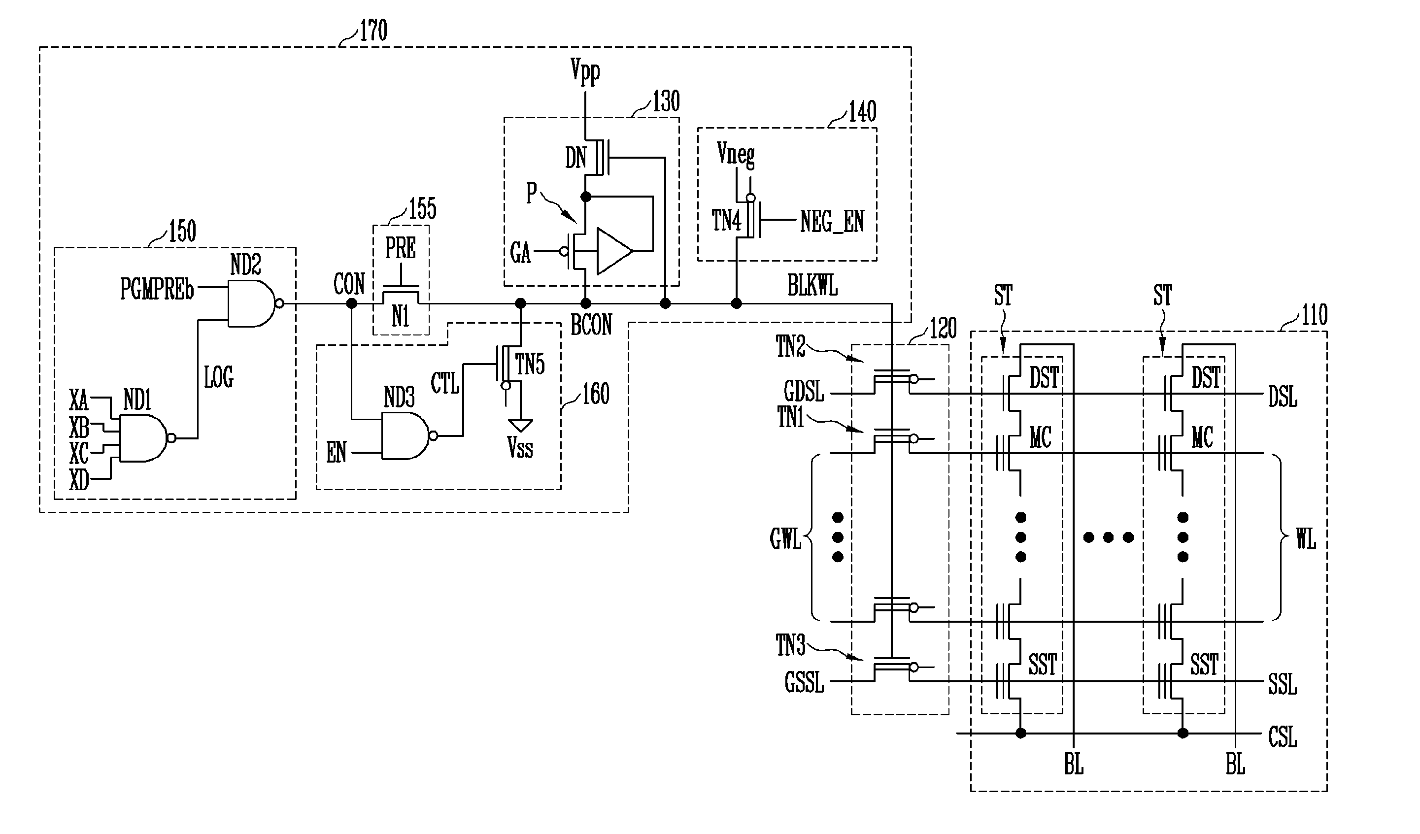
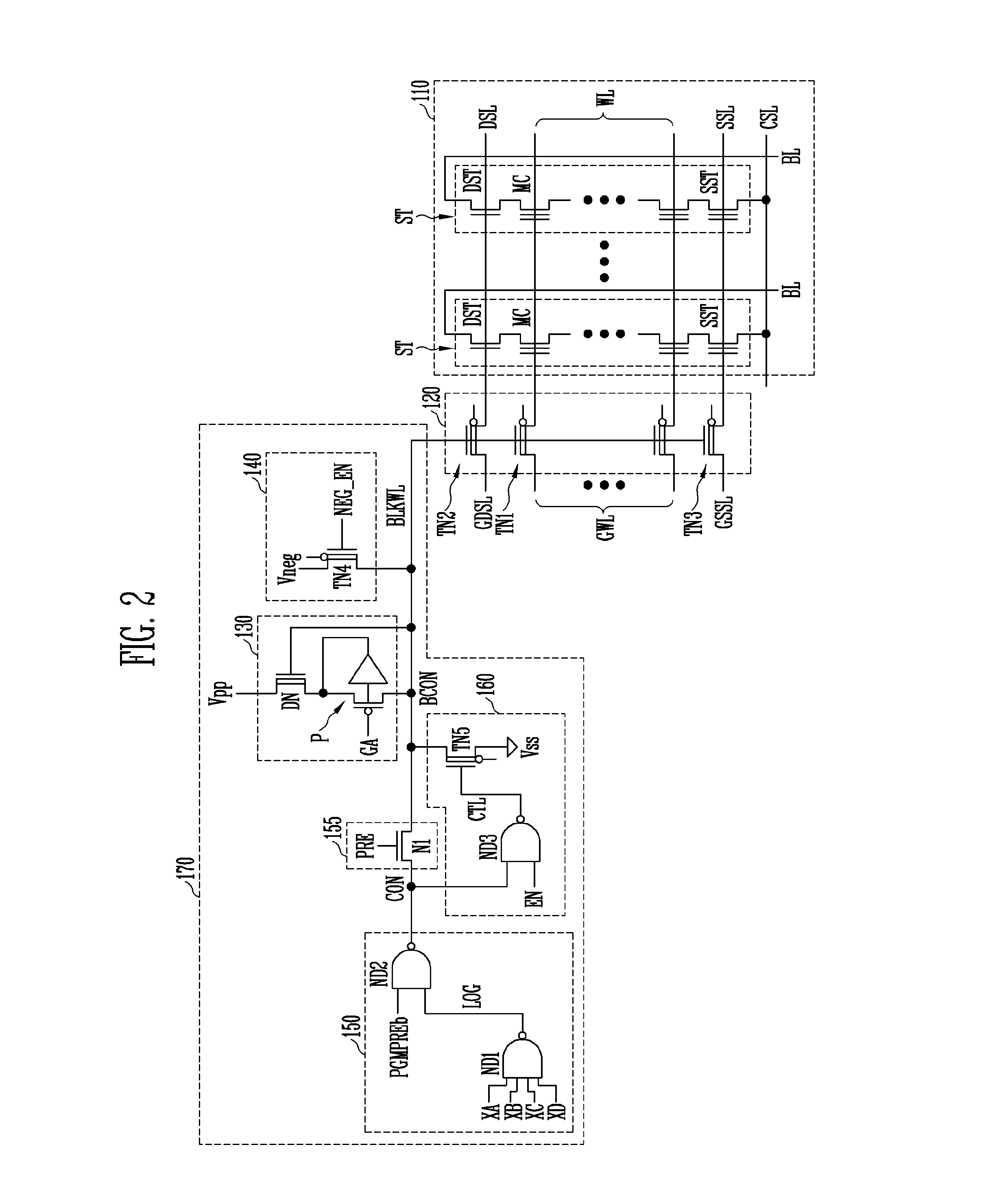
[0028]Hereinafter, some exemplary embodiments of the present disclosure will be described in detail with reference to the accompanying drawings. The figures are provided to allow those having ordinary skill in the art to understand the scope of the embodiments of the disclosure.

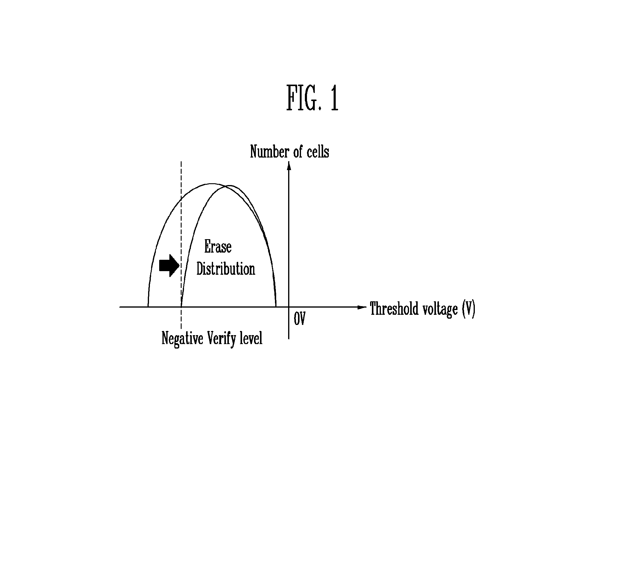
[0029]FIG. 1 illustrates one example of the threshold voltage distribution of memory cells in an erase state.

[0030]Referring to FIG. 1, a negative threshold voltage is associated with each of the memory cells in an erase state. In a program operation, the threshold voltage of a program state, which is higher than the threshold voltage of an erase state, is associated with each of the memory cells. When the erase state threshold voltage distribution of the memory cells is not made sufficiently narrow, there may be present a less-than-sufficient margin between the threshold voltage distributions of a program state. In order to secure the margin between the threshold voltage distributions of the memory cells in ...


PUM


Abstract

A memory device includes a block switch for transferring operating voltages, supplied to global lines, to local lines coupled to a memory cell array in response to the voltage level of a block selection signal and a negative voltage transfer circuit for transferring a negative voltage as the block selection signal in order to couple the global lines and the local lines when the operating voltage has a negative level and to disconnect the global lines and the local lines from each other when the block selection signal is disabled.

Description

CROSS-REFERENCE TO RELATED APPLICATION[0001]Priority is claimed to Korean patent application number 10-2010-0085444 filed on Sep. 1, 2010, the entire disclosure of which is incorporated herein by reference in its entirety.BACKGROUND[0002]Exemplary embodiments relate to a semiconductor memory device and more particularly to securing sufficient margin between threshold voltage distributions in a semiconductor memory device.[0003]Data storage capacity of a memory device can be increased by configuring each memory cell to store more than one bit. There then could be four or more distributions of memory cell threshold voltages. There may be three or more distributions of threshold voltages of the memory cells in a program state as well as the distribution of threshold voltages of memory cells in an erase state. These distributions must be secured with a sufficient margin between them in order to determine without error as to which distribution of what state belongs the certain threshold ...

Claims


Application Information

Patent Timeline
Patent Type & Authority Patents(United States)
IPC IPC(8): G11C16/06
CPCG11C16/08G11C17/165G11C17/18
Inventor KOO, MIN GYU
Owner SK HYNIX INC
Why Eureka
Try Eureka