Photo mask

a mask and photo technology, applied in the field of photo masks, can solve the problems of short channel effect, degrade refresh characteristics and reliability of semiconductor devices,

Inactive Publication Date: 2006-10-19
SK HYNIX INC
View PDF2 Cites 1 Cited by
  • Summary
  • Abstract
  • Description
  • Claims
  • Application Information

AI Technical Summary

Benefits of technology

[0015] Accordingly, it is an object of the present invention to provide a photo mask for forming a STAR gate region including a H-type light-shield pattern in an exposure process so as to prevent collapse of an etching mask pattern or a gate in a process for forming a STAR gate and secure a margin of the exposure process.

Problems solved by technology

In general, due to high-integration of a semiconductor device, a gate having a stacked structure causes a problem such as a short channel effect.
However, when the etching mask pattern for forming a STAR gate region is formed, an etching mask pattern is collapsed or a gate leaning phenomenon occurs to degrade refresh characteristics and reliability of the semiconductor device.

Method used


Image

  • Photo mask
  • Photo mask
  • Photo mask

Examples


Embodiment Construction

[0022] The present invention will be described in detail with reference to the accompanying drawings. Wherever possible, the same reference numbers will be used throughout the drawings to refer to the same or like parts. It should be appreciated that the embodiments are provided for the purpose that one ordinarily skilled in the art would be able to understand the present invention, and modifications in various manners and the scope of the present invention are not limited by the embodiments described herein.

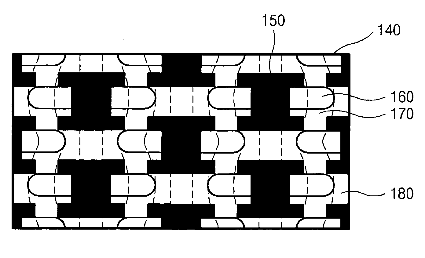
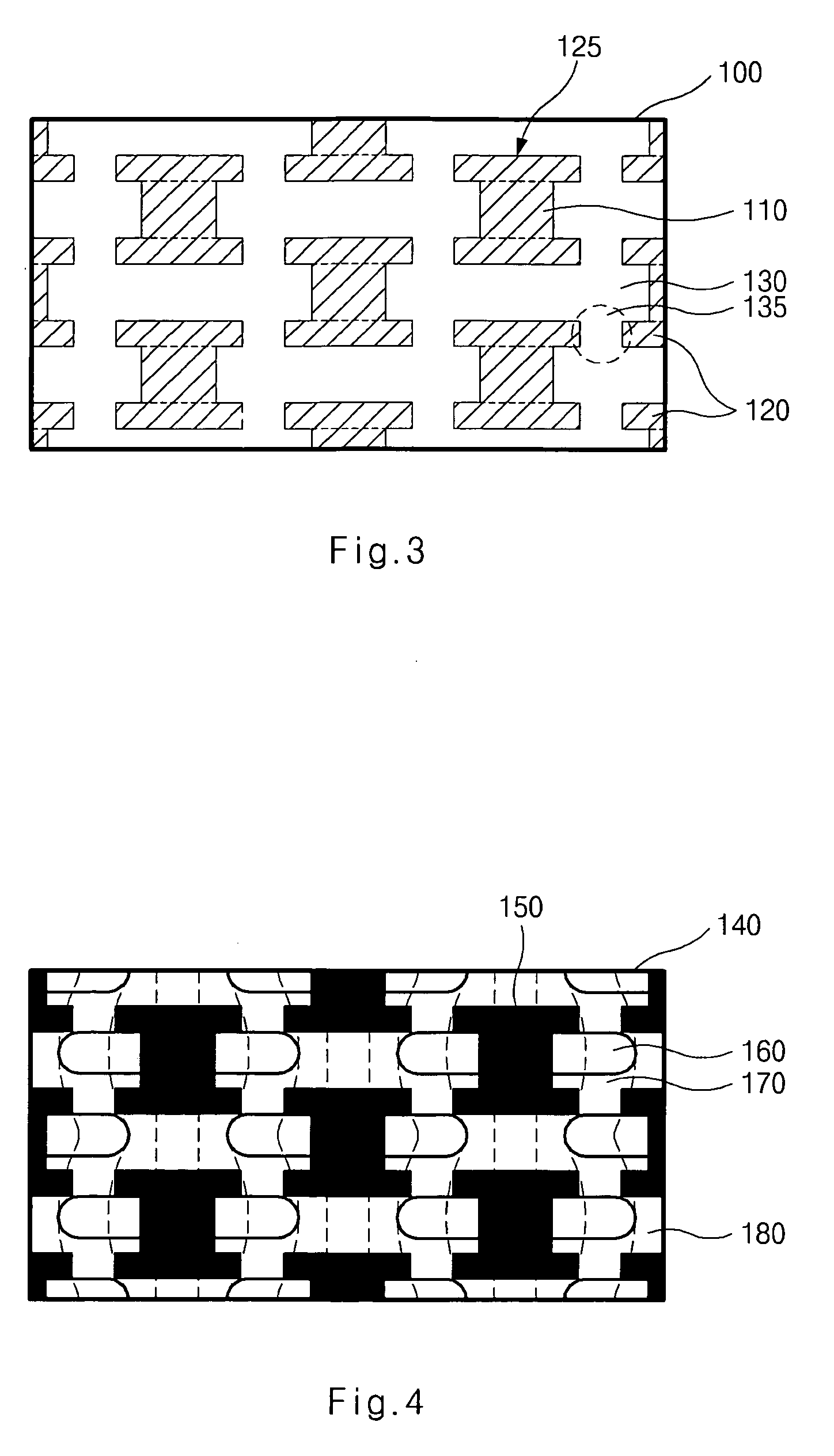
[0023]FIG. 3 is a simplified plane view illustrating a photo mask according to an embodiment of the present invention.

[0024] Referring to FIG. 3, the photo mask comprises a H-type light-shield pattern 125 and a light-transmission pattern 130, wherein the H-type light-shield patterns are alternately arranged on a transparent substrate 100, and elsewhere the light-transmission pattern 130. The H-type light-shield pattern 125 corresponds to an etching mask pattern on a semiconduc...


PUM

PropertyMeasurementUnit
distanceaaaaaaaaaa
aspect ratioaaaaaaaaaa
distanceaaaaaaaaaa

Abstract

A photo mask comprises a H-type light-shield pattern. In an exposure process, a photo mask is used to form a STAR (Step Asymmetry Recess) gate region, thereby stably securing a storage node contact region and improving a refresh characteristic of a semiconductor device.

Description

BACKGROUND OF THE INVENTION [0001] 1. Field of the Invention [0002] The present invention generally relates to a photo mask, and more specifically, to a photo mask including a H-type light-shield pattern used in order to form a STAR gate region in an exposure process, thereby securing a storage node contact region and improving refresh characteristics of a semiconductor device. [0003] 2. Description of the Related Art [0004] In general, due to high-integration of a semiconductor device, a gate having a stacked structure causes a problem such as a short channel effect. [0005] In order to overcome the problem, a transistor having a Step Asymmetry Recessed (hereinafter, referred to as “STAR”) Cell Scheme has been suggested. The transistor having a STAR cell structure increases a channel length as a transistor having a structure where a step difference is formed in a gate region to overcome the short channel effect. [0006] In one process for forming a STAR gate, a device isolation film ...

Claims


Application Information

Patent Timeline
Patent Type & Authority Applications(United States)
IPC IPC(8): G03C7/26G03C1/08G03C7/32
CPCG03F1/14G03F1/00G03F1/54
Inventor BAE, SANG MANPARK, DONG HEOK
Owner SK HYNIX INC
Why Eureka
Try Eureka