

GOA drive unit and GOA drive circuit
a technology of drive circuit and drive unit, which is applied in the field of drive technology of display panel, can solve the problems of high risk of efficacy loss, severe influence on and the efficacy loss so as to reduce the efficacy loss risk of the tft device and improve the reliability of the goa drive circui
- Summary
- Abstract
- Description
- Claims
- Application Information
AI Technical Summary
Benefits of technology
Problems solved by technology
Method used
Image

Examples
embodiment 1
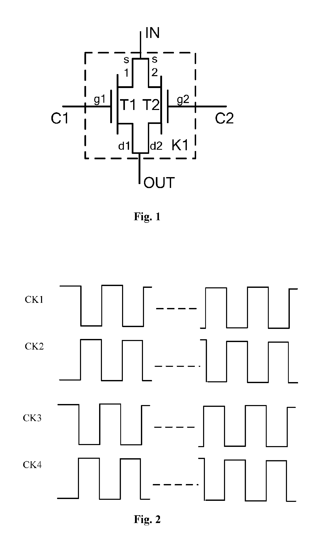
[0040]FIG. 1 is a structural diagram of a bidirectional selection unit in a GOA drive unit according to a specific embodiment of the present disclosure. As shown in FIG. 1, the bidirectional selection unit comprises a first switching element K1, which has a first control end C1, a second control end C2, a signal input end IN, and a signal output end OUT.
[0041]Furthermore, the first switching element K1 includes two parallel TFT devices. As shown in FIG. 1, a first thin film transistor T1 and a second thin film transistor T2 constitute two parallel transmission channels, respectively. A source s1 of T1 is connected to a source s2 of T2, serving as the signal input end IN of the first switching element K1. A drain d1 of T1 is connected to a drain d2 of T2, serving as the signal output end OUT of the first switching element K1. A gate g1 of T1 serves as the first control end C1 of the first switching element K1; and a gate g2 of T2 serves as the second control end C2 of the first switc...
embodiment 2
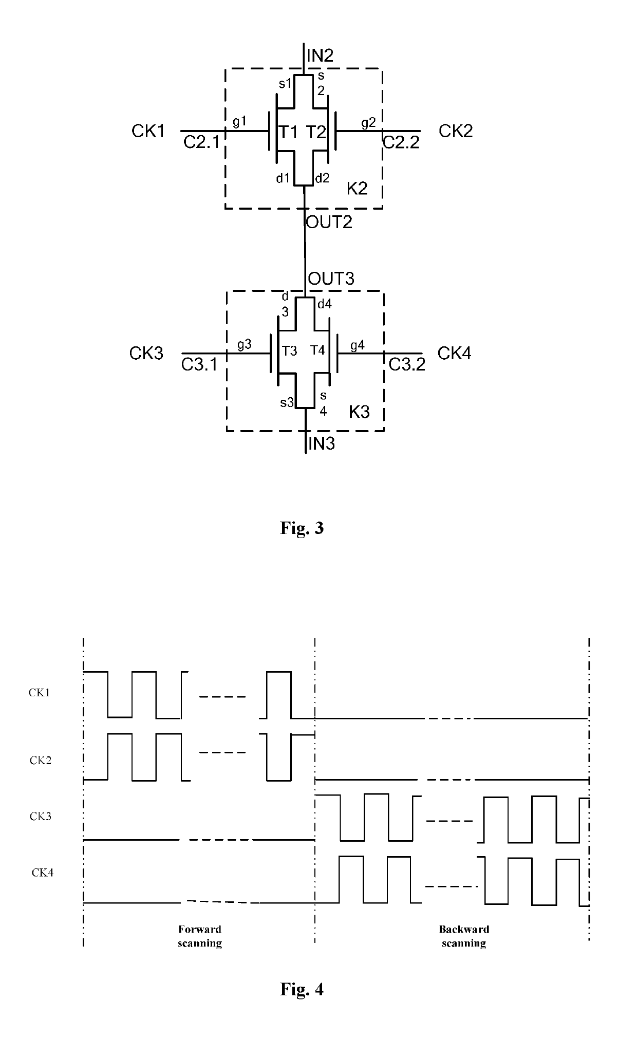
[0051]FIG. 3 is a structural diagram of a bidirectional selection unit in a GOA drive unit based on another embodiment of the present disclosure. As shown in FIG. 3, the bidirectional selection unit comprises a second switching element K2 and a third switching element K3. The second switching element K2 has a first control end C2.1, a second control end C2.2, a signal input end IN2, and a signal output end OUT2. The third switching element K3 has a first control end C3.1, a second control end C3.2, a signal input end IN3, and a signal output end OUT3.
[0052]Furthermore, each of the second switching element K2 and the third switching element K3 includes two parallel TFT devices. As shown in FIG. 3, the second switching element K2 comprises a first thin film transistor T1 and a second thin film transistor T2, which constitute two parallel transmission channels, respectively. A source s1 of T1 is connected to a source s2 of T2, serving as the signal input end IN2 of the second switching...
PUM
 Abstract
Description
Claims
Application Information