Electronic device including fingerprint recognition module provided with conductive pattern

a fingerprint recognition and electronic device technology, applied in the field of electronic devices including fingerprint recognition modules provided with conductive patterns, can solve the problems of increasing the amount of power consumed by electronic devices, inconvenience for users, etc., and achieve the effects of reducing manufacturing costs, reducing the number of electronic components, and reducing power consumption

Active Publication Date: 2021-10-26
SAMSUNG ELECTRONICS CO LTD
View PDF17 Cites 0 Cited by
  • Summary
  • Abstract
  • Description
  • Claims
  • Application Information

AI Technical Summary

Benefits of technology

[0008]With an electronic device according to various example embodiments, the touch panel and the fingerprint sensor are activated when a user's finger approaches an area in which a fingerprint sensor is disposed, making it possible to minimize and / or reduce power consumption.
[0009]With an electronic device according to various example embodiments, instead of implementing an always-on-display (AOD), it is possible to activate the fingerprint recognition icon via the display based on a user's finger being located within a specified vicinity of the fingerprint sensor. Thus, it is possible to reduce the number of electronic components for implementing the AOD, and thus it is possible to reduce manufacturing costs.

Problems solved by technology

A conventional fingerprint sensor is disposed in an area exposed to the exterior of an electronic device, a button or an area of a housing to receive a user's fingerprint, and input from the button or one area of the rear housing may be unintuitive or may cause inconvenience to the user.
When the fingerprint sensor and the touch screen panel (TSP) are constantly activated, the amount of power consumed by the electronic device may increase.

Method used


Image

  • Electronic device including fingerprint recognition module provided with conductive pattern
  • Electronic device including fingerprint recognition module provided with conductive pattern
  • Electronic device including fingerprint recognition module provided with conductive pattern

Examples


Embodiment Construction

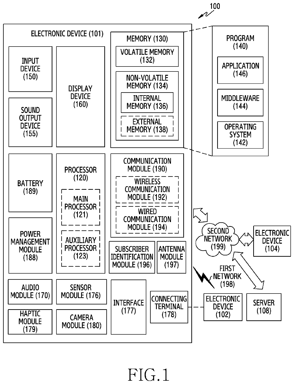
[0026]FIG. 1 is a block diagram illustrating an example electronic device in a network environment according to an exemplary embodiment.

[0027]FIG. 1 is a block diagram illustrating an electronic device 101 in a network environment 100 according to various embodiments. Referring to FIG. 1, the electronic device 101 in the network environment 100 may communicate with an electronic device 102 via a first network 198 (e.g., a short-range wireless communication network), or an electronic device 104 or a server 108 via a second network 199 (e.g., a long-range wireless communication network). According to an embodiment, the electronic device 101 may communicate with the electronic device 104 via the server 108. According to an embodiment, the electronic device 101 may include a processor 120, memory 130, an input device 150, a sound output device 155, a display device 160, an audio module 170, a sensor module 176, an interface 177, a haptic module 179, a camera module 180, a power manageme...


PUM


Abstract

Disclosed is an electronic device. An electronic device according to various embodiments may include: a housing including a front face and a rear face opposite the front face; a transparent plate defining the front face of the housing; a display panel disposed below the transparent plate; a fingerprint sensor disposed between the display panel and the rear face of the housing and configured to acquire biometric information about an external object that is within a specified proximity of the transparent plate; and a conductive pattern disposed adjacent to the fingerprint sensor and configured to detect whether the external object is within a specified proximity of the fingerprint sensor.

Description

CROSS-REFERENCE TO RELATED APPLICATION[0001]This application is based on and claims priority under 35 U.S.C. § 119 to Korean Patent Application No. 10-2018-0159914, filed on Dec. 12, 2018, in the Korean Intellectual Property Office, the disclosure of which is incorporated by reference herein in its entirety.BACKGROUND1) Field[0002]The disclosure relates to an electronic device including a fingerprint recognition module provided with a conductive pattern.2) Description of Related Art[0003]An electronic device, which is versatile, may store various types of personal information, and may have an authentication function using biometric information such as a fingerprint or an iris of a user as a means for financial transactions or personal authentication. The importance of authentication services is increasing for the protection of personal information when using financial transactions or authentication services. As the fingerprint sensor, at least one of a capacitive fingerprint sensor,...

Claims


Application Information

Patent Timeline
Patent Type & Authority Patents(United States)
IPC IPC(8): G06K9/00G06F3/041G06F21/32G06V40/13
CPCG06K9/00026G06F3/041G06F21/32G06K9/00053G06F1/1626G06F1/1684G06V40/13G06F2203/04103G06F1/1643G06F1/1696H05K2201/05G06V40/12G06V40/1335G06V40/1329
Inventor KIM, JONGDOOCHO, JAEROKJU, WANJAE
Owner SAMSUNG ELECTRONICS CO LTD
Why Eureka
Try Eureka