Method of and an arrangement for analyzing manufacturing defects of multi-chip modules made without known good die

a technology of manufacturing defects and multi-chip modules, applied in the direction of electronic circuit testing, measurement devices, instruments, etc., can solve the problems of inability to cost-effectively streamline the mcm manufacturing process, and inability to meet the requirements of jtag compliant devices. to achieve the effect of eliminating guesswork

Active Publication Date: 2022-04-05
WANG PETER SHUN SHEN
View PDF23 Cites 0 Cited by
  • Summary
  • Abstract
  • Description
  • Claims
  • Application Information

AI Technical Summary

Benefits of technology

[0009]An objective of the present invention is to provide a dependable method and arrangement for boundary scan testing and debugging, in order to eliminate guesswork in making MCMs and to get away from pre-packaging of IC dice.
[0031]The present invention provides a reliable method and arrangement for boundary scan testing and debugging newly manufactured multi-chip modules (MCMs) made to identical design specifications with no KGDs therein. Advantageously, a first and a second MCM are temporarily linked in tandem for boundary scan testing by a motherboard serially daisy-chaining their internal dice, and interlinking the corresponding boundary scan cells of the first and second MCM to approach parallel buses, assisted by a switch on the motherboard, to (1) run self-test or mutual test through bidirectional chain reactions in order to generate an extended Truth Table that includes an array of combined netlist, and (2) to map out test vectors as “1” and “0” in response of High and Low per Drive and Sense, to thereby diagnose mismatched bits according to the preset test patterns. Any disagreement between the first MCM and the second MCM on the Truth Table would indicate error bits occurred at their linked nets. Further failure analysis provides an opportunity for trouble-shooting bad dice, and to solve many faults ranging from nets, pins to the substrate, which may be reworked by, e.g., a reflowing process to solve problems related to Known Bad Die at certain interconnections in especially the flip chips depending on issues concerning bumping, soldering pads, etc. due to cold or hot soldering. Further inventive method includes applying analog and digital methods to avoid misjudgment on or misdiagnosis of good dice if mixed boundary scan cells include a number of linkage bits in one pin of a particular die. This inventive method could distinguish some pins for boundary scan from the other pins designed for functional test to thereby determine and conclude that a newly made module is a Known Good Module (KGM) without KGD. This KGM can then be used to create additional KGMs from other unknown Modules in accordance with the present invention.

Problems solved by technology

This process is time consuming and expensive and is generally only suitable for single die package.
However, the advent of multi-chip modules (MCMs) renders this methodology impractical, if not obsolete.
Given the increasingly compact 3D packaging of bare dice in an MCM without KGD, chip manufacturers cannot cost-effectively streamline their MCM manufacturing process in order to validate and guarantee the quality of MCMs.
Heretofore, there is no prior art solution to the problem of making reliable MCMs via a novel application of tandem mode testing and debugging, without requiring KGDs in a mass production environment.

Method used


Image

  • Method of and an arrangement for analyzing manufacturing defects of multi-chip modules made without known good die
  • Method of and an arrangement for analyzing manufacturing defects of multi-chip modules made without known good die
  • Method of and an arrangement for analyzing manufacturing defects of multi-chip modules made without known good die

Examples


Embodiment Construction

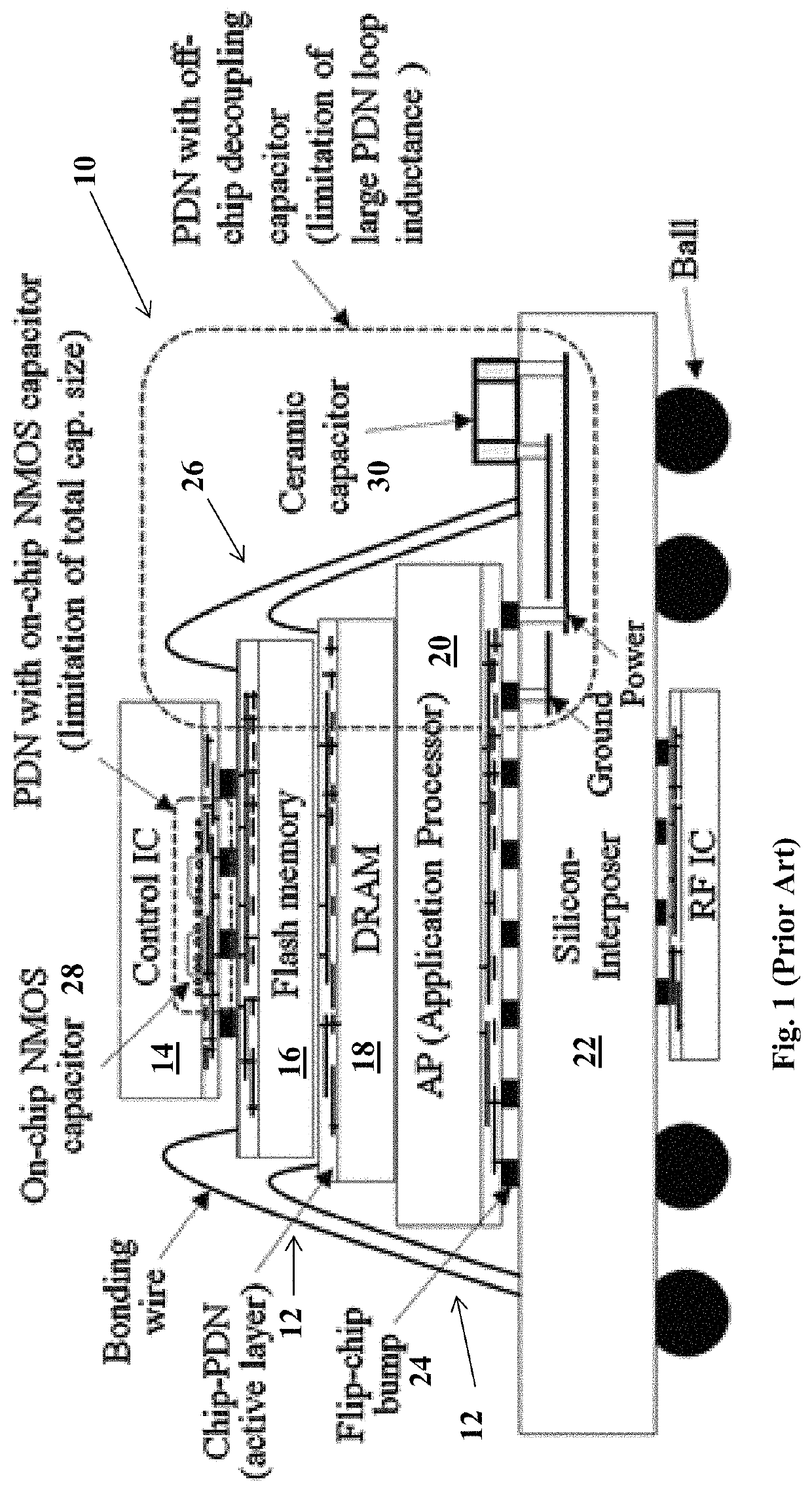
[0058]FIG. 1 shows an exemplary 3D architecture of a multi-chip module (MCM) 10 having a plurality of dice 12 stacked atop each other: a control integrated circuit (IC) 14, a Flash memory 16, a dynamic random-access memory (DRAM) 18, and an Application Processor (AP) 20, all of which sit atop a silicon interposer 22 via flip-chip bumping 24. Wire bonding 26 may be used to selectively connect these dice and discrete components such as, for example, N-type metal-oxide-semiconductor (NMOS) 28 or ceramic capacitors 30. The 3D architecture design also contemplates stacked dice and / or stacked memories selectively placed across and interconnected to each other through the silicon interposer for signal communications as well as grounding and power. This entire assembly may be flip-chip mounted onto a package substrate, preferably made of polyimide having a high dielectric constant, and housed in a suitable package (which may be referred to as a Ball Grid Array (BGA) package). Designers of S...


PUM


Abstract

The present invention provides a reliable method and arrangement for boundary scan testing and debugging newly manufactured multi-chip modules (MCMs) made to identical design specifications with no Known Good Die therein. Advantageously, a first and a second MCM are temporarily linked in tandem for boundary scan testing through a motherboard and daisy-chaining their internal dice, and interlinking the corresponding boundary scan cells of the identical dice of the first and second MCM to (1) run self-test on individual MCMs and mutual test on the MCMs connected in tandem in order to generate an extended Truth Table that includes responses from an array of combined netlists of the first and second MCMs, and (2) to diagnose mismatched bits in the extended Truth Table using a Boundary Scan Diagnostics software so as to identify defects in the first and second MCMs.

Description

CROSS REFERENCES TO RELATED APPLICATIONS[0001]This application claims priority from U.S. Provisional Application No. 62 / 924,488 filed on Oct. 22, 2019 and U.S. Provisional Application No. 62 / 975,835 filed on Feb. 13, 2020, the disclosure of which is incorporated herein by reference in its entirety.FIELD OF INVENTION[0002]The present invention relates to the field of determining manufacturing defects of JTAG compliant devices, and more particularly, to a method and an arrangement for analyzing manufacturing defects in multi-chip modules (MCMs) made without known good die (KGD) by innovatively linking two or more MCMs in tandem and boundary scan testing the linked MCMs in a repetitive and reciprocal manner.BACKGROUND OF THE INVENTION[0003]It has been a common practice in the semiconductor chip manufacturing industry to fully test dice prior to their chip packaging onto circuit boards in order to avoid costly return of merchandise. A “Known Good Die” (KGD) is a fully tested chip prior ...

Claims


Application Information

Patent Timeline
Patent Type & Authority Patents(United States)
IPC IPC(8): G01R31/3177G01R31/317G01R31/3183G01R31/3185G01R31/28
CPCG01R31/3177G01R31/2815G01R31/3183G01R31/31705G01R31/31723G01R31/318508G01R31/318533G01R31/318597G01R31/318513G01R31/318566G01R31/318538
Inventor WANG, PETER SHUN SHEN
Owner WANG PETER SHUN SHEN
Why Eureka
Try Eureka