Fingerprint module includes identification components in an identification area and a chip disposed in a nonidentification area and display device

a fingerprint module and chip technology, applied in the field of fingerprint module and display device, can solve the problems of inflexibility, increase the cost of the display device, and the inability to identify fingerprints on the fingerprint identification device, so as to reduce the frame of the display device and increase the screen ratio

Active Publication Date: 2022-04-12
WUHAN CHINA STAR OPTOELECTRONICS TECH CO LTD
View PDF9 Cites 0 Cited by
  • Summary
  • Abstract
  • Description
  • Claims
  • Application Information

AI Technical Summary

Benefits of technology

[0020]In summary, beneficial effects of the embodiment of the present disclosure are as follows. Compared with the prior art, in order to solve the above technical problems, the fingerprint module and the display device of the embodiment of the present disclosure can increase a fingerprint identification area and achieve full-screen fingerprint identification through the fingerprint identification components disposed in the identification area of the substrate and the fingerprint chip disposed in a non-identification area of the substrate. In addition, the embodiment of the present disclosure can effectively reduce the frame of the display device, which is beneficial to the display device to increase a screen ratio and beneficial to a full screen design.

Problems solved by technology

The fingerprint identification can only be done on the fingerprint identification device and is limited to within the limited area of 10 mm2 of the frame, which is not flexible.
In addition, additional fingerprint identification device increases the cost of the display device and increase the frame size of the display device.

Method used


Image

  • Fingerprint module includes identification components in an identification area and a chip disposed in a nonidentification area and display device
  • Fingerprint module includes identification components in an identification area and a chip disposed in a nonidentification area and display device

Examples


Embodiment Construction

[0024]The following description of the various embodiments is provided to illustrate the specific embodiments.

[0025]The embodiments described herein with reference to the accompanying drawings are explanatory, illustrative, and used to generally understand the present disclosure. Furthermore, directional terms described by the present disclosure, such as top, bottom, front, back, left, right, inner, outer, side, etc., are only directions by referring to the accompanying drawings, and thus the used terms are used only for the purpose of describing embodiments of the present disclosure and are not intended to be limiting of the present disclosure.

[0026]In the drawings, modules with similar structures are labeled with the same reference number.

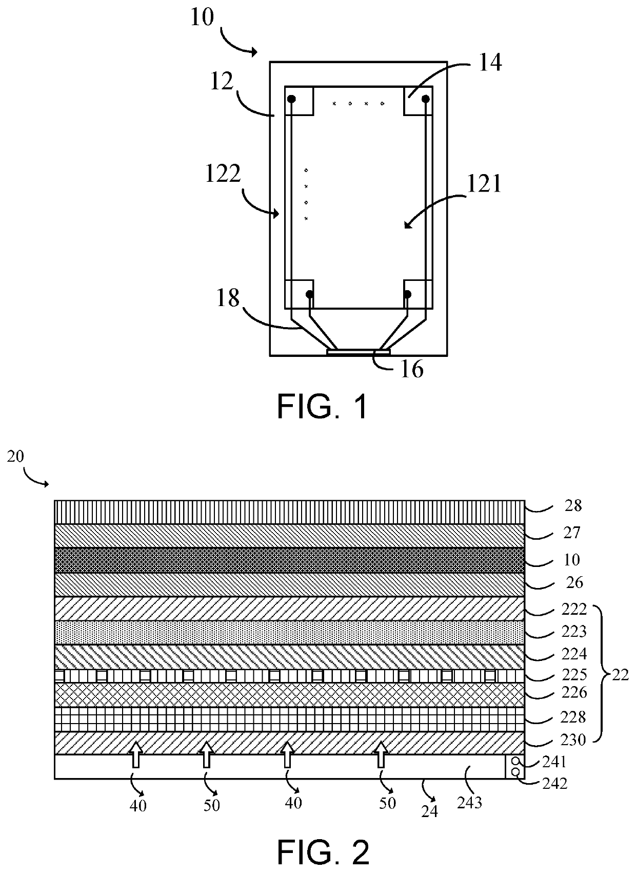
[0027]Refer to FIG. 1, a schematic structural view of a fingerprint module according to an embodiment of the present disclosure is provided.

[0028]Referring to FIG. 1, in an embodiment of the present disclosure, a fingerprint module 10 includes a ...


PUM

PropertyMeasurementUnit
areaaaaaaaaaaa
capacitanceaaaaaaaaaa
identification areaaaaaaaaaaa

Abstract

A fingerprint module includes a substrate, a plurality of fingerprint identification components, a fingerprint chip, and a plurality of metal wires. The substrate has an identification area configured to identify a fingerprint and a non-identification area located at a periphery of the identification area. The fingerprint identification components are disposed in the identification area of the substrate. The fingerprint chip is disposed in a non-identification area of the substrate. Each of the fingerprint identification components is electrically connected to the fingerprint chip through a corresponding metal wire.

Description

FIELD OF INVENTION[0001]The present disclosure relates to the field of fingerprint identification technologies, and more particularly to a fingerprint module and a display device.BACKGROUND OF INVENTION[0002]Fingerprints are textures formed by an uneven skin on fingertips of human fingers. Capacitive fingerprint identification is based on capacitance differences induced by depressed skin and raised skin of fingertips. By collecting the capacitance differences induced by the fingers pressing on a fingerprint reader, shapes of the fingerprints can be restored and fingerprint identification can be performed.[0003]In the prior art, a technical solution of fingerprint identification provides adding a fingerprint identification device on a front surface or a back surface of a frame of the display device. The frame has, for example, a limited area of 10 mm2. The fingerprint identification device has a small identification area. The fingerprint identification can only be done on the fingerp...

Claims


Application Information

Patent Timeline
Patent Type & Authority Patents(United States)
IPC IPC(8): G06F3/042G06F3/041G02F1/1333G06F3/03G06F3/047G06V40/13
CPCG06F3/0421G02F1/13338G06F3/0325G06F3/047G06F3/04164G06V40/1318
Inventor HUANG, CHUNHUNGHUANG, YAOLIHE, XINGLONG
Owner WUHAN CHINA STAR OPTOELECTRONICS TECH CO LTD
Why Eureka
Try Eureka