Display panel, display screen, and electronic device

a display panel and electronic device technology, applied in the field of display technology, can solve the problems of large borders and large width achieve the effects of reducing the frame of the display panel, reducing the number of data lines, and reducing the width of the region where fan-out lines are located

Inactive Publication Date: 2022-01-06
WUHAN CHINA STAR OPTOELECTRONICS SEMICON DISPLAY TECH CO LTD
View PDF1 Cites 0 Cited by
  • Summary
  • Abstract
  • Description
  • Claims
  • Application Information

AI Technical Summary

Benefits of technology

[0008]The display panel, the display screen, and the electronic device the embodiment of the present disclosure comprises the non-shared pixel array consisting of the plurality of non-shared pixels, wherein the non-shared pixel array comprises the plurality of non-shared pixel columns and the plurality of non-shared pixel rows, the shared pixel array consisting of the plurality of shared pixels, wherein the shared pixel array comprises the plurality of shared pixel columns and the plurality of shared pixel rows, the shared pixel columns are disposed between the two adjacent non-shared pixel columns, and the shared pixel rows are disposed between the two adjacent non-shared pixel rows, the plurality of data lines, wherein the non-shared pixel row and the shared pixel column adjacent to the non-shared pixel row correspond to one data line, and the plurality of scanning lines, wherein the non-shared pixel column and the shared pixel column respectively correspond to one scanning line. Since the number of data lines is reduced, a width of a region where fan-out lines are located is reduced, thereby reducing the frame of the display panel.

Problems solved by technology

However, in current Pentile arrangement of pixels, each row of pixels corresponds to a data line, that is, a greater number of data lines results in a greater width of a region where fan-out lines between a display region and a driving chip, which results in a larger borders of a display panel.

Method used


Image

  • Display panel, display screen, and electronic device
  • Display panel, display screen, and electronic device
  • Display panel, display screen, and electronic device

Examples


Embodiment Construction

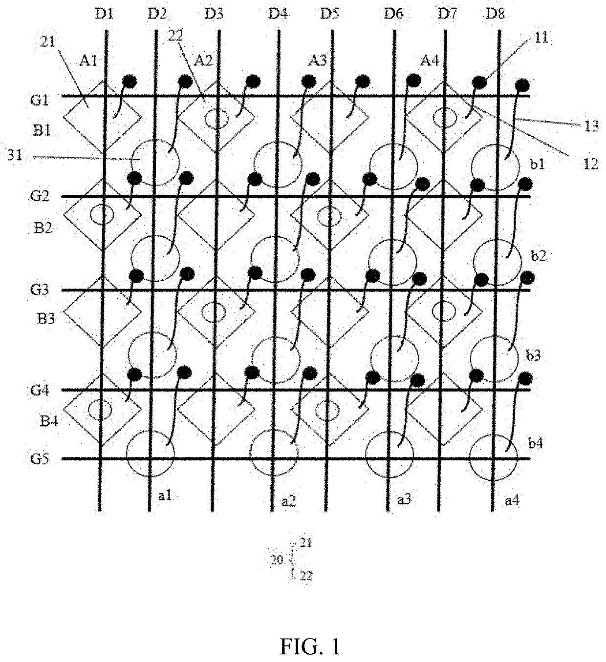
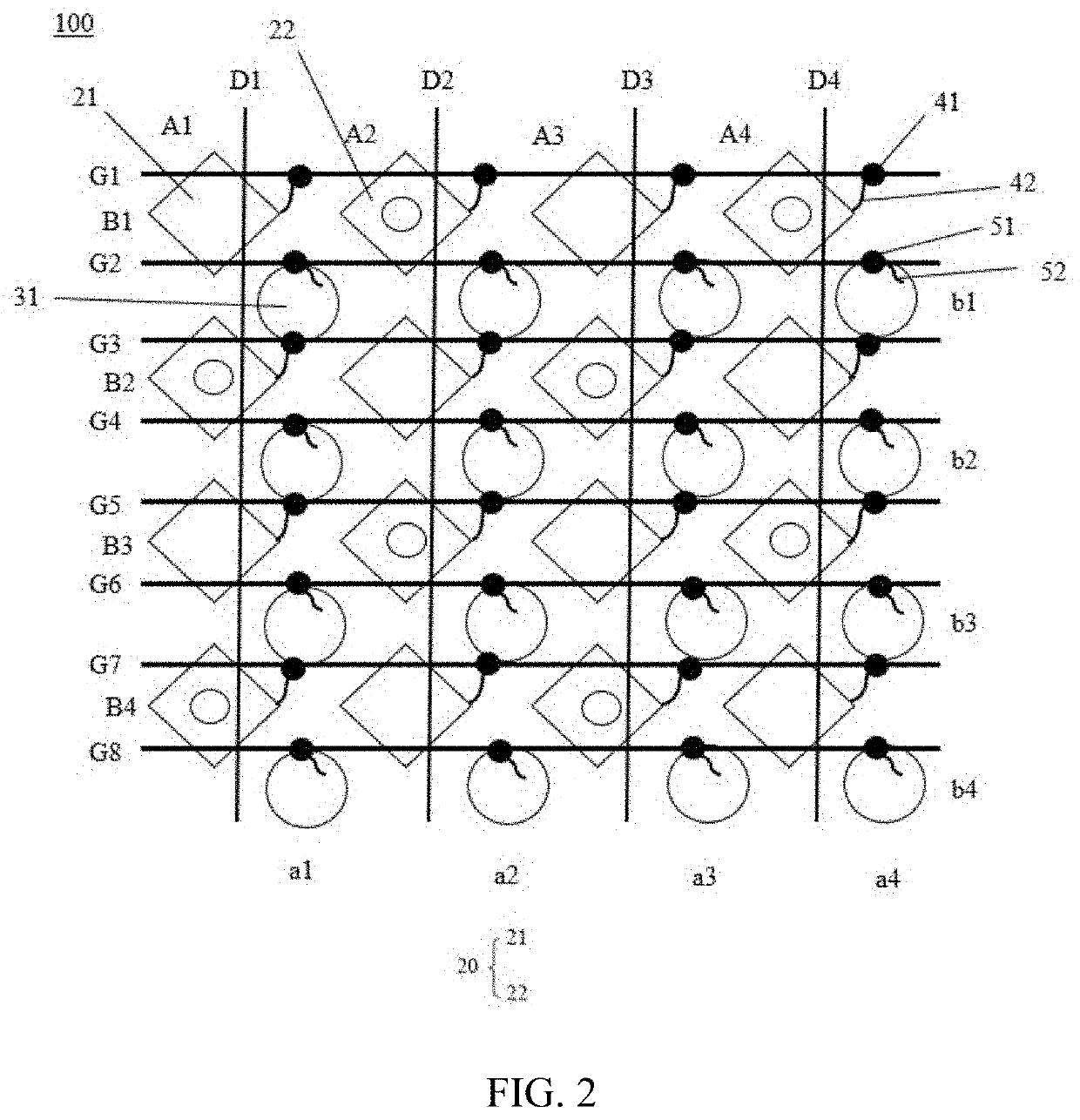
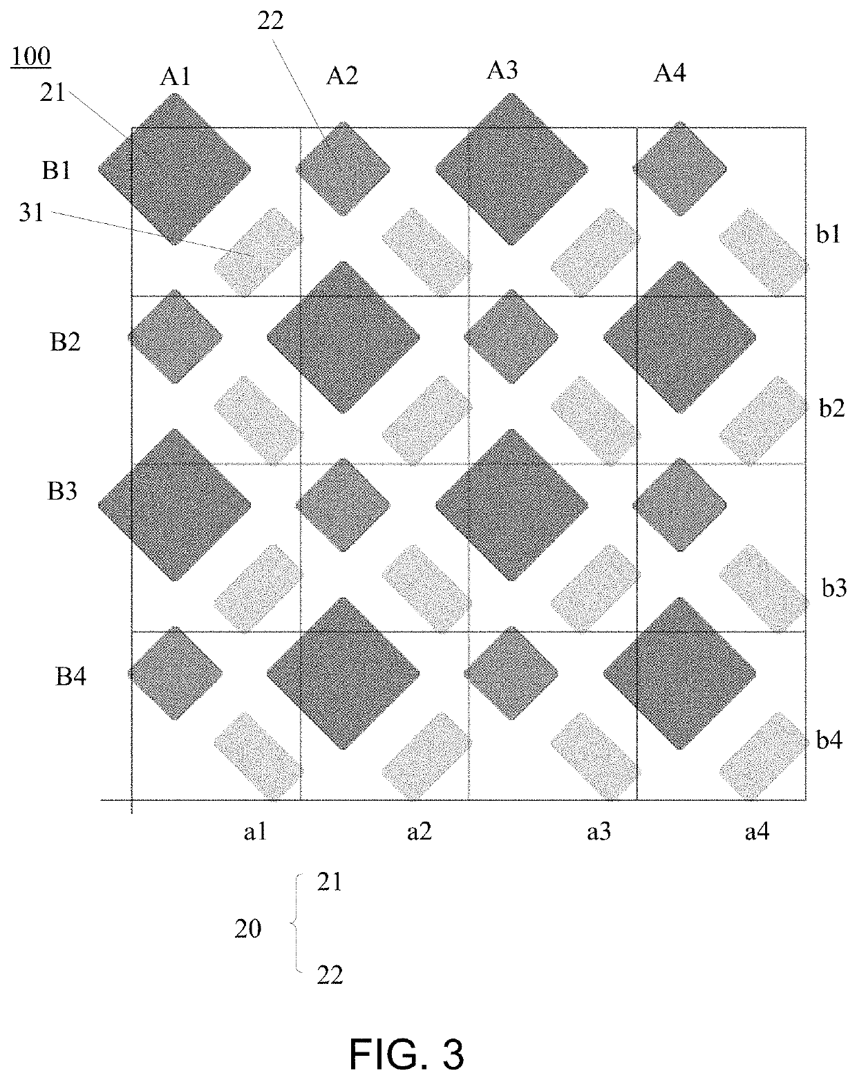
[0015]The technical solutions in the embodiments of the present disclosure will be clearly and completely described below in conjunction with accompanying drawings in the embodiments of the present disclosure. Obviously, the embodiments described are merely a part of the present disclosure, rather than all the embodiments. All other embodiments obtained by the person having ordinary skill in the art based on embodiments of the disclosure, without making creative efforts, are within the scope of the present disclosure.

[0016]In descriptions of the present disclosure, it should be noted that, orientations or position relationships indicated by the terms, such as “center”, “longitudinal”, “transverse”, “length”, “width”, “thickness”, “upper”, “lower”, “front”, “back”, “left”, “right”, “vertical”, “horizontal”, “top”, “bottom”, “inside”, “outside”, “clockwise”, “counterclockwise”, etc. are based on the orientations or position relationships shown in the drawings. These are only convenien...


PUM


Abstract

The present invention provides a display panel, a display screen, and an electronic device. The display panel includes a non-shared pixel array including a plurality of non-shared pixel columns and a plurality of non-shared pixel rows, a shared pixel array including a plurality of shared pixel columns and a plurality of shared pixel rows, and a plurality of data lines, wherein the non-shared pixel row and the shared pixel column adjacent to the non-shared pixel row correspond to one data line.

Description

FIELD OF INVENTION[0001]The present disclosure relates to the field of display technology, and more particularly, to a display panel, a display screen, and an electronic device.BACKGROUND OF INVENTION[0002]A structure of small and medium-sized organic light-emitting diode display devices is mainly composed of a driving backplane and pixels (organic light-emitting diodes) with a specific arrangement structure. A brightness of each organic light-emitting diode is individually controlled by an output current of a driving circuit unit, and a pixel array consisting of organic light-emitting diodes with different light-emitting colors is controlled by a corresponding drive circuit, to finally realize an output of images.[0003]However, in current Pentile arrangement of pixels, each row of pixels corresponds to a data line, that is, a greater number of data lines results in a greater width of a region where fan-out lines between a display region and a driving chip, which results in a larger...

Claims


Application Information

Patent Timeline
Patent Type & Authority Applications(United States)
IPC IPC(8): G09G3/3208H01L27/32
CPCG09G3/3208G09G2330/028G09G2300/0439H01L27/3276G09G2300/0452G09G2300/0426G09G2300/0465H10K59/352H10K59/353H10K59/179H10K59/131
Inventor ZHOU, SHANG
Owner WUHAN CHINA STAR OPTOELECTRONICS SEMICON DISPLAY TECH CO LTD
Why Eureka
Try Eureka