PUF-film and method for producing the same

a technology of film and film, applied in the direction of transmission, internal/peripheral component protection, instruments, etc., can solve the problems of hsm's data not being decrypted by the adversary, the cryptographic key is permanently lost, and the battery-backed system cannot be fully recovered, so as to maintain the accuracy of measurements, hamper the diversification of structures, and high apparatus security

Active Publication Date: 2022-04-12
FRAUNHOFER GESELLSCHAFT ZUR FOERDERUNG DER ANGEWANDTEN FORSCHUNG EV
View PDF45 Cites 0 Cited by
  • Summary
  • Abstract
  • Description
  • Claims
  • Application Information

AI Technical Summary

Benefits of technology

[0013]According to an embodiment of the first aspect, a method for producing a PUF-film comprises printing a layer of dielectric material on a film substrate, such that a variable thickness of the layer is obtained by the printing. The method comprises arranging a structured electrode layer on the dielectric material. The method is executed such that the structured electrode layer is influenced with respect to an electric measurement value due to the variable thickness. This allows for generating a PUF by use of a printing process so as to obtain simple and robust PUF-films using reliable processes.
[0061]According to an embodiment of the third aspect, the apparatus comprises a housing. The PUF-film comprises a sensor region being formed by an overlap region of first circuit elements in a first trace layer and second circuit elements in a second trace layer. The housing is completely covered by the sensor region. This allows for a high security of the apparatus. According to an embodiment of the third aspect, the PUF-film comprises a carbon material at least partially covering the circuit elements, wherein the PUF-film is covered with an electric shield comprising a metallic mesh or a sprayed conductive layer. The carbon material may comprise a same or within a tolerance range of 10% same absorption coefficient when compared to the conductive traces and / or the shield at least in the relevant optical regions such as X-ray and / or visible wavelength. This allows for hampering diversification of structures because the traces become hardly or impossibly distinguishable from the carbon material such that the traces may become invisible. The carbon material may optionally allow for at least a degree of opaqueness in the visible wavelength range and the x-ray wavelength range. The low conductive property may be at least partially compensated with the electric shield so as to maintain the preciseness of the measurements.

Problems solved by technology

As a drawback, the battery-backed system is (i.e., during storage and transport) in operation.
As any intrusion destroys parts of the enclosure, the cryptographic key is permanently lost and the HSM's data cannot be decrypted by the adversary after intrusion.
It verifies the enclosure's integrity but does not provide PUF readout.
Since its integrity verification method is based on a Wheatstone bridge, it can hardly be integrated into a PUF measurement system as both methods would interfere with each other.
Despite employing capacitive sensing for detecting intruding objects, it cannot extract capacitive PUF properties.
Despite that this circuit concept can extract PUF properties, it is not compatible with a large-scale enclosure and also does not support integrity verification.
Similar issues are observed for the BoardPUF [5] which uses a capacitive PUF, implemented in the printed circuit board (PCB) but has no means for integrity verification.
Furthermore, protecting embedded devices against physical attacks is a challenging task since the attacker has control of the device in a hostile environment.
However, the battery affects the system's robustness and weight and also leads to difficulties with the security mechanism while shipping the device.
While single-chip devices such as smartcards can be protected in silicon, multiple-chip embedded systems on Printed Circuit Boards (PCBs) can only be secured with an additional physical security boundary that separates the secure and insecure domains of a system.
Attempts to penetrate the mesh are very likely to destroy its tracks and result in open circuits.
This approach has significant practical drawbacks: adding a battery to the system increases bulk and weight, it lowers its robustness with regard to the operating temperature range, and prohibits prolonged storage.
When the battery is fully discharged, the CSPs are lost and physical integrity can no longer be guaranteed [8].
Moreover, storing CSPs in a BBRAM leaves room for the zeroization circuit to fail.
However, storing a key in a non-volatile memory is also not an option, as its contents can be extracted while the system is powered off [9].
As long as the device is powered off, extracting these parameter is supposedly difficult.
Since most PUFs are implemented in Integrated Circuits (IC), it is impossible to use them for aftermarket protection of Commercial-Off-The-Shelf (COTS) components.
Furthermore, silicon based PUFs typically do not have the property of tamper-evidence [11].
I.e., once powered on, they cannot verify if an attack was executed on the system while powered off.
Even worse, they are incapable of detecting online attacks that extract values during runtime [12].
This allows for producing robust and reliable PUF-films as drilling through the PUF-film destroys the granule leading to defects being difficult to be repaired.
This allows for hampering diversification of structures because the traces become hardly or impossibly distinguishable from the carbon material such that the traces may become invisible.

Method used


Image

  • PUF-film and method for producing the same
  • PUF-film and method for producing the same
  • PUF-film and method for producing the same

Examples


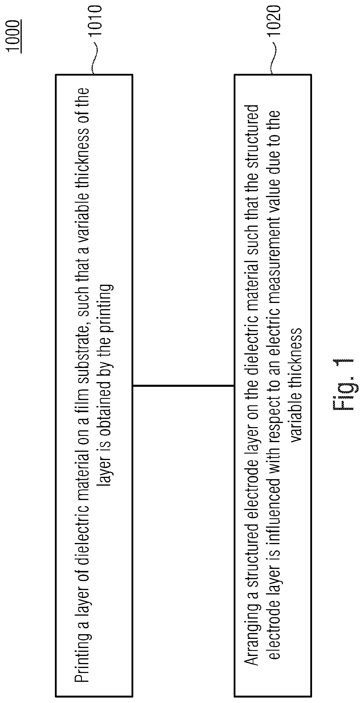
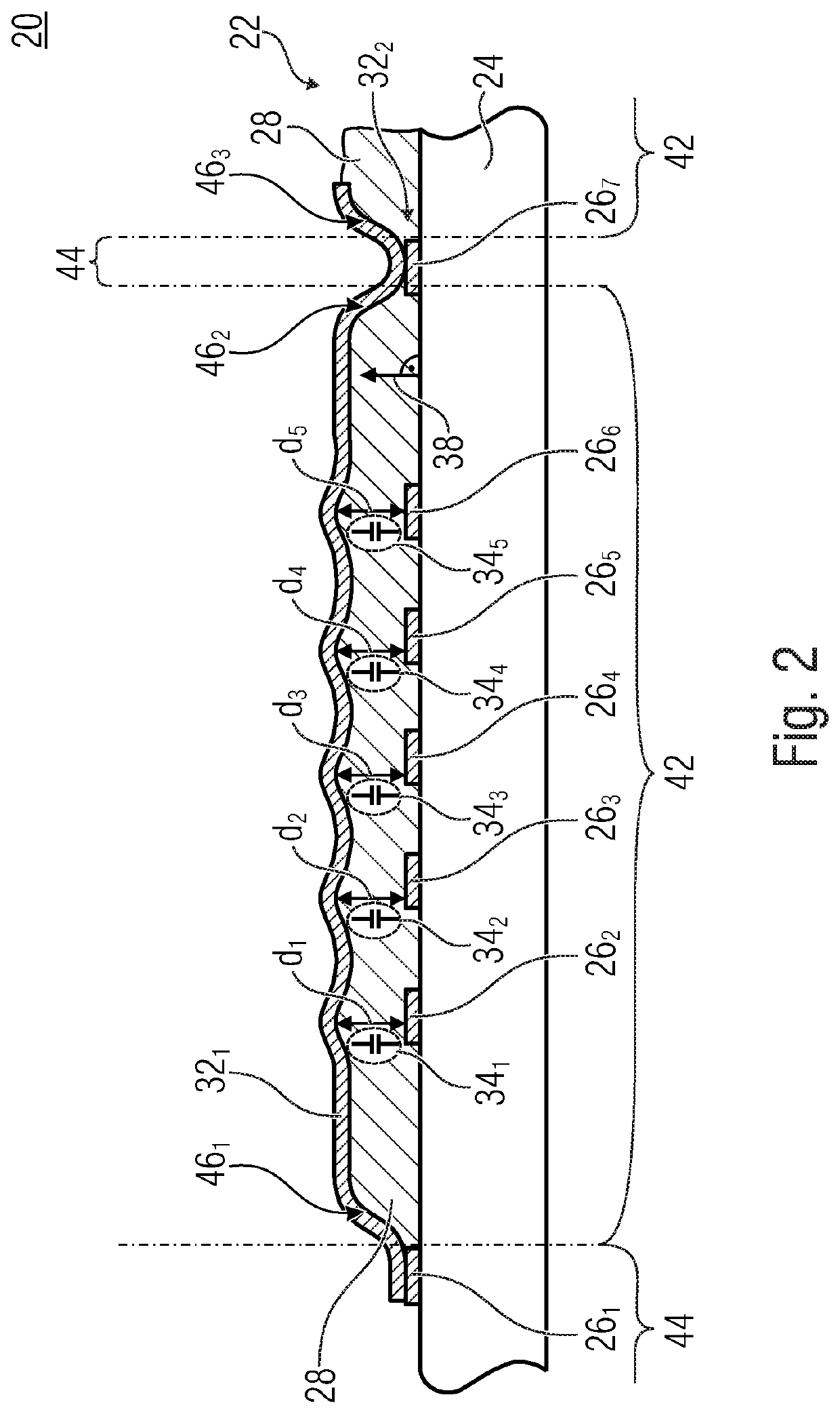
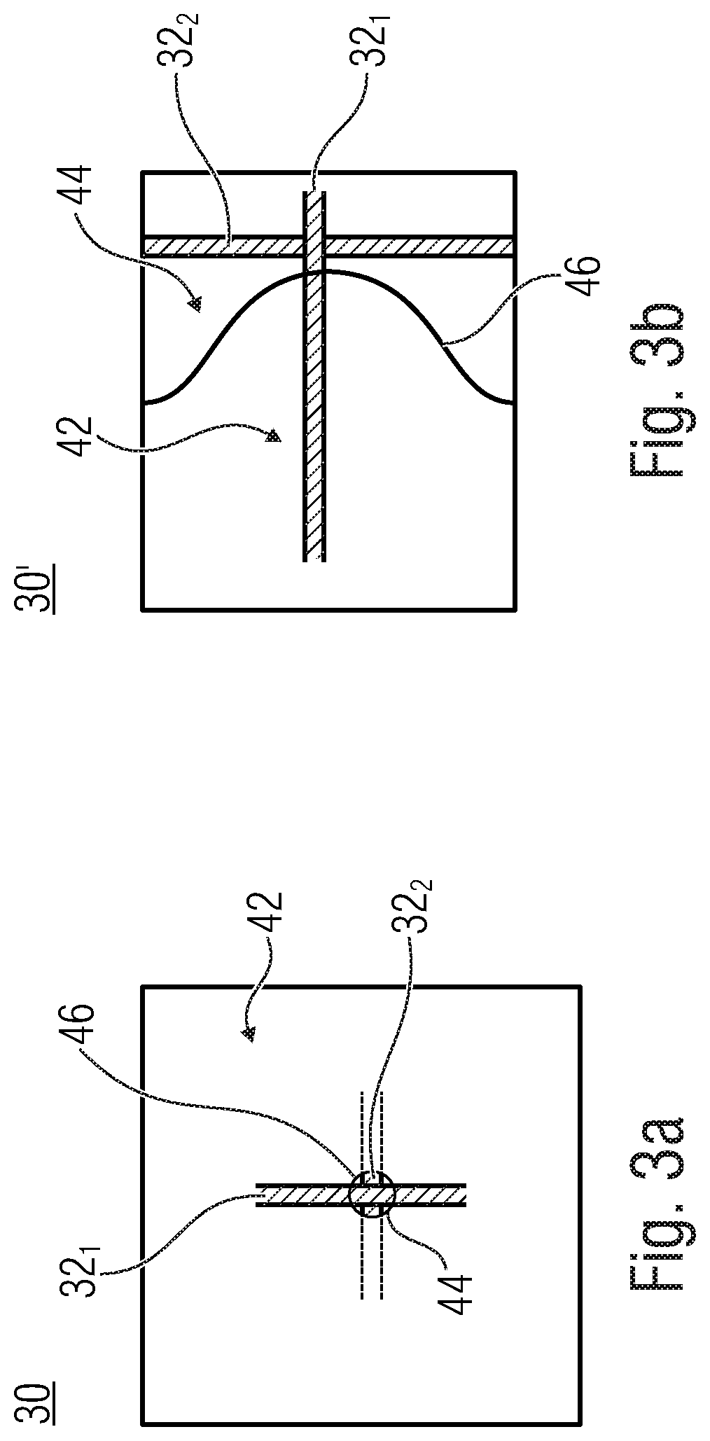
Embodiment Construction

[0110]Equal or equivalent elements or elements with equal or equivalent functionality are denoted in the following description by equal or equivalent reference numerals even if occurring in different figures.

[0111]In the following description, a plurality of details is set forth to provide a more thorough explanation of embodiments of the present invention. However, it will be apparent to those skilled in the art that embodiments of the present invention may be practiced without these specific details. In other instances, well-known structures and devices are shown in block diagram form rather than in detail in order to avoid obscuring embodiments of the present invention. In addition, features of the different embodiments described hereinafter may be combined with each other, unless specifically noted otherwise.

[0112]In the following, reference is made to Physically Unclonable Functions (PUFs). In connection with the embodiments described hereinafter, PUFs are understood as electri...


PUM

PropertyMeasurementUnit
diameteraaaaaaaaaa
diameteraaaaaaaaaa
diameteraaaaaaaaaa

Abstract

A PUF-film includes a flat circuit structure including a plurality of circuit elements and includes a flat electric shield. The circuit structure is evaluable with respect to a plurality of electric capacitance values being arranged between the plurality of circuit elements. The electric shield at least partially covers the circuit structure and provides for a counter reference electrode of the plurality of electric capacitance values.

Description

CROSS-REFERENCE TO RELATED APPLICATION[0001]This application claims priority from European Patent Application No. 18166145.5, which was filed on Apr. 6, 2018, and is incorporated herein in its entirety by this reference thereto.[0002]The present invention relates to PUF-films and to a method for producing the same. The present invention further relates to a method for producing a capacitive foil array using a dielectric layer effecting a capacitive variation and, at the same time, enables a via-free foil architecture. The present invention further relates to a circuit concept for monitoring a protective housing on a basis of a capacitive PUF-structure with a further possibility for integrity checks. The present invention further relates to a concept for a protective housing on a basis of a capacitive PUF-structure with a possibility for integrity checks including an optional embedding of a security sensor and layout randomization. Security enclosures that are permanently monitored f...

Claims


Application Information

Patent Timeline
Patent Type & Authority Patents(United States)
IPC IPC(8): G06F21/87H04L9/32H05K1/02H04L9/08G09C1/00
CPCG06F21/87G09C1/00H04L9/0866H04L9/3278H05K1/0231H04L2209/12
Inventor IMMLER, VINCENTOBERMAIER, JOHANNES
Owner FRAUNHOFER GESELLSCHAFT ZUR FOERDERUNG DER ANGEWANDTEN FORSCHUNG EV
Why Eureka
Try Eureka