

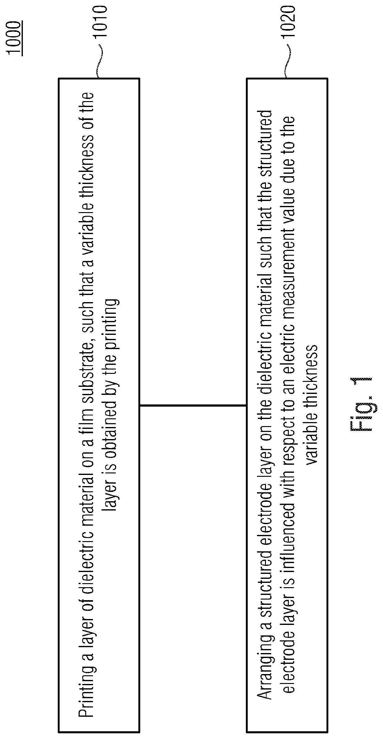
PUF-film and method for producing the same
a technology of film and film, applied in the direction of digital transmission, securing communication, and the details of semiconductor/solid-state devices, can solve the problems of inability to recover sensitive data, unbalanced measured capacitance value, and opaqueness
- Summary
- Abstract
- Description
- Claims
- Application Information
AI Technical Summary
Benefits of technology
Problems solved by technology
Method used
Image

Examples
Embodiment Construction
[0110]Equal or equivalent elements or elements with equal or equivalent functionality are denoted in the following description by equal or equivalent reference numerals even if occurring in different figures.
[0111]In the following description, a plurality of details is set forth to provide a more thorough explanation of embodiments of the present invention. However, it will be apparent to those skilled in the art that embodiments of the present invention may be practiced without these specific details. In other instances, well-known structures and devices are shown in block diagram form rather than in detail in order to avoid obscuring embodiments of the present invention. In addition, features of the different embodiments described hereinafter may be combined with each other, unless specifically noted otherwise.
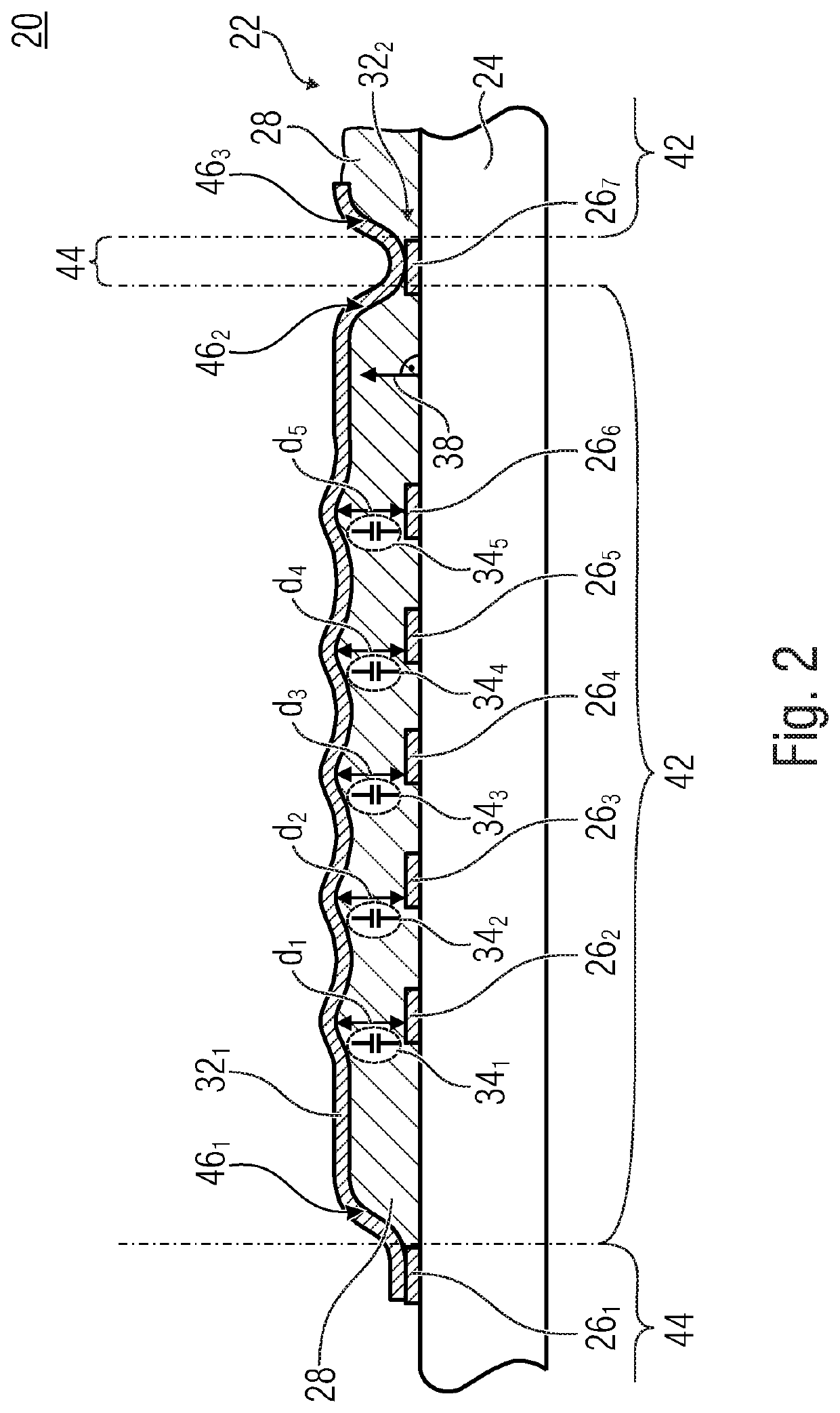
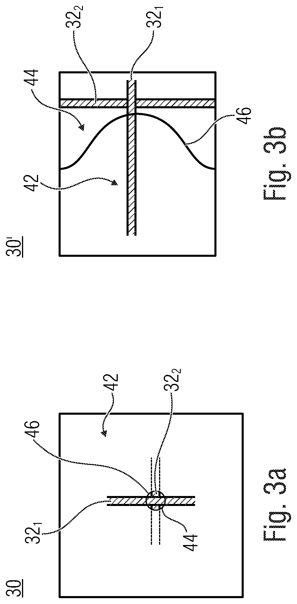
[0112]In the following, reference is made to Physically Unclonable Functions (PUFs). In connection with the embodiments described hereinafter, PUFs are understood as electri...
PUM
| Property | Measurement | Unit |
|---|---|---|
| diameter | aaaaa | aaaaa |
| diameter | aaaaa | aaaaa |
| diameter | aaaaa | aaaaa |
Abstract
Description
Claims
Application Information