Electronic component and manufacturing method for the same
a manufacturing method and technology for electronic components, applied in the field of electronic components, can solve the problems of shrinkage of the soldering and risk of a crack being generated in the electronic componen
- Summary
- Abstract
- Description
- Claims
- Application Information
AI Technical Summary
Benefits of technology
Problems solved by technology
Method used
Image
Examples
first preferred embodiment
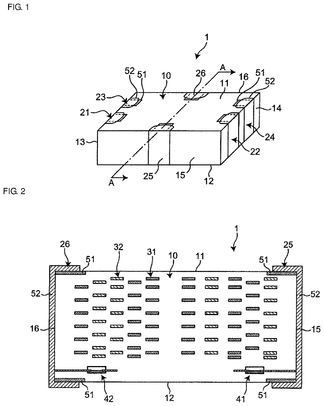
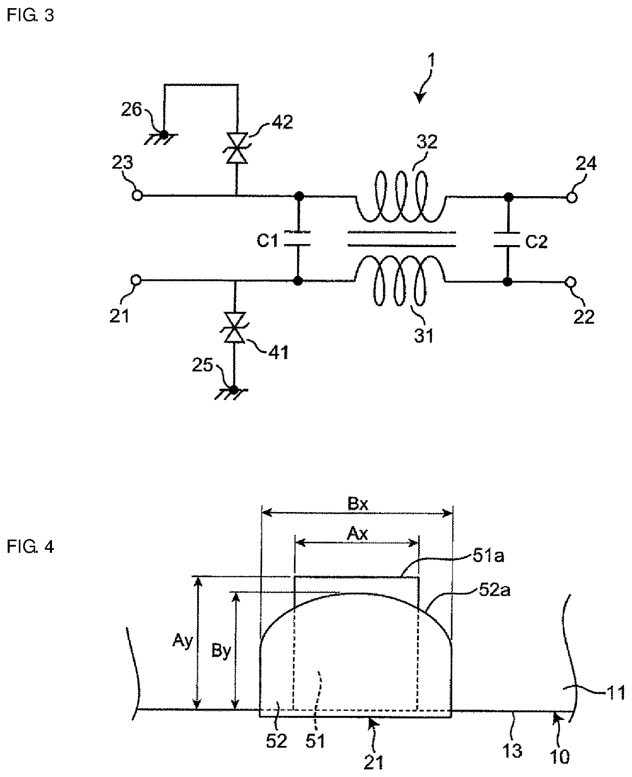
[0075]FIG. 1 is a perspective view illustrating a first preferred embodiment of an electronic component of the present invention. FIG. 2 is a cross-sectional view taken along a line A-A in FIG. 1. As illustrated in FIG. 1 and FIG. 2, an electronic component 1 is a common mode choke coil including an ESD protection element. The electronic component 1 includes an element body 10, a first coil 31 and a second coil 32 provided inside the element body 10, a first discharge element 41 and a second discharge element 42 provided inside the element body 10, and first to sixth outer electrodes 21 to 26 provided in or on the element body 10.
[0076]The element body 10 includes a top surface 11, a bottom surface 12 opposing the top surface 11, and first to fourth side surfaces 13 to 16 connecting the top surface 11 and the bottom surface 12. The first side surface 13 and the second side surface 14 oppose each other, and the third side surface 15 and the fourth side surface 16 oppose each other. T...
second preferred embodiment
[0102]FIG. 8 is a cross-sectional view illustrating a second preferred embodiment of an electronic component of the present invention. The thickness of a lower layer electrode in the second preferred embodiment differs from the thickness of the lower layer electrode in the first preferred embodiment. The above-described different configuration will be described below. Since the remaining configuration is the same or substantially the same as that of the first preferred embodiment, the same reference signs as those in the first preferred embodiment are assigned thereto, and description thereof will be omitted.
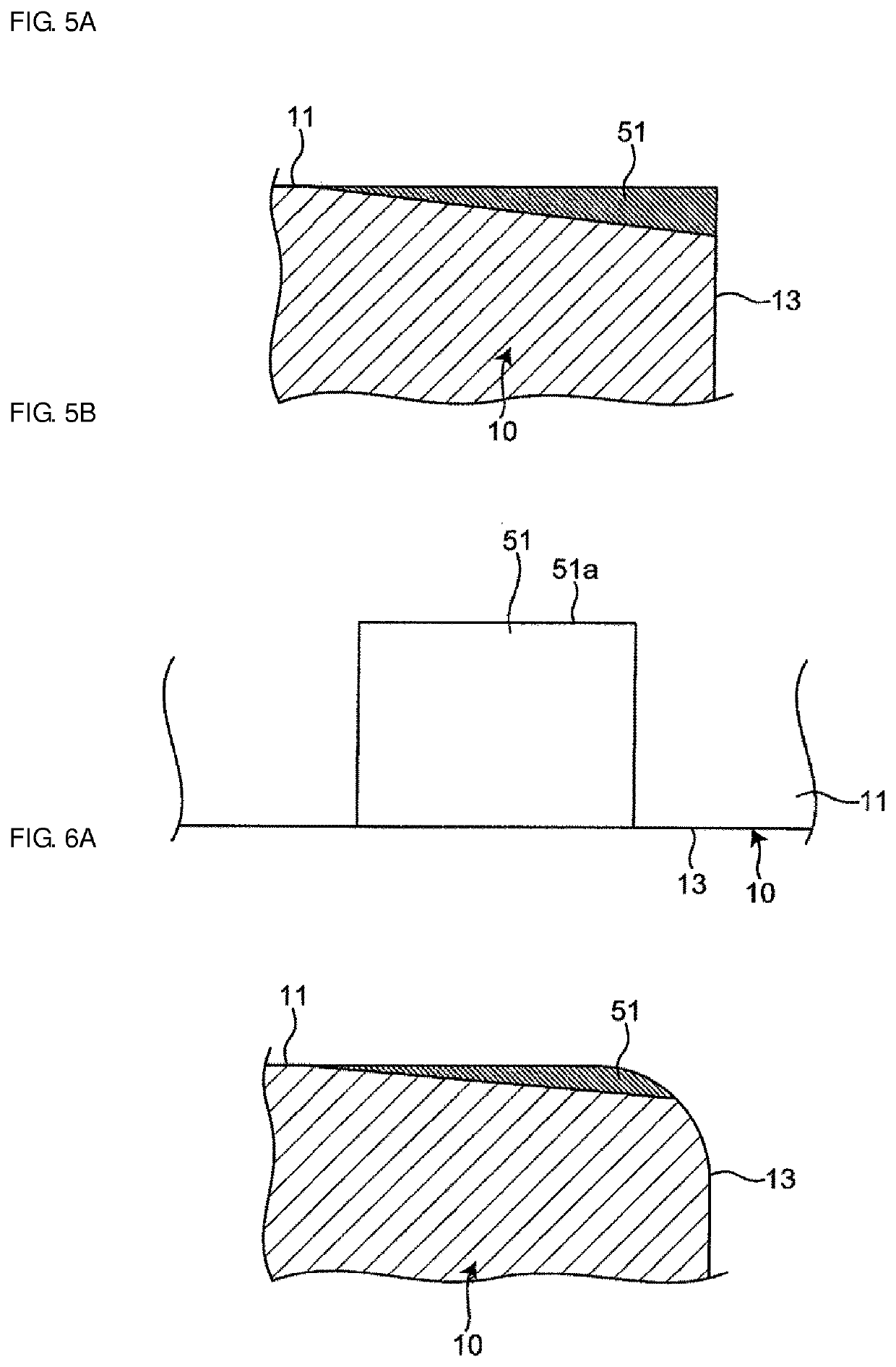
[0103]As illustrated in FIG. 8, in an electronic component 1A of the second preferred embodiment, in a cross section at the center or approximate in a width direction of a lower layer electrode 51, the thickness of the lower layer electrode 51 is thicker toward a side surface 13. As discussed in the first preferred embodiment, the width direction is a direction along the first s...
third preferred embodiment
[0112]FIG. 10 is a cross-sectional view illustrating a third preferred embodiment of an electronic component of the present invention. A state of an interface between a lower layer electrode and an upper layer electrode in the third preferred embodiment differs from that in the first preferred embodiment. The above-described different configuration will be described below. The remaining configuration is the same or substantially the same as that of the first preferred embodiment, and description thereof will be omitted.
[0113]As illustrated in FIG. 10, in an electronic component 1B of the third preferred embodiment, an upper layer electrode 52 and a lower layer electrode 51 include contact surfaces 52c and 51c, respectively, having a convexo-concave shape. The contact surface 52c of the upper layer electrode 52 and the contact surface 51c of the lower layer electrode 51 are in close contact with each other with substantially no gaps therebetween. Thus, the upper layer electrode 52 an...
PUM
| Property | Measurement | Unit |
|---|---|---|
| relative dielectric constant εr | aaaaa | aaaaa |
| thickness | aaaaa | aaaaa |
| average particle diameter | aaaaa | aaaaa |
Abstract
Description
Claims
Application Information


