Multilayer ceramic capacitor
a ceramic capacitor and multi-layer technology, applied in the direction of fixed capacitor details, fixed capacitors, printed circuit non-printed electric components association, etc., can solve the problems of cracking, no consideration is given to suppress the occurrence of cracks caused by internal stress, etc., to reduce or prevent the occurrence of cracks
- Summary
- Abstract
- Description
- Claims
- Application Information
AI Technical Summary
Benefits of technology
Problems solved by technology
Method used
Image
Examples
embodiment 1
Preferred Embodiment 1
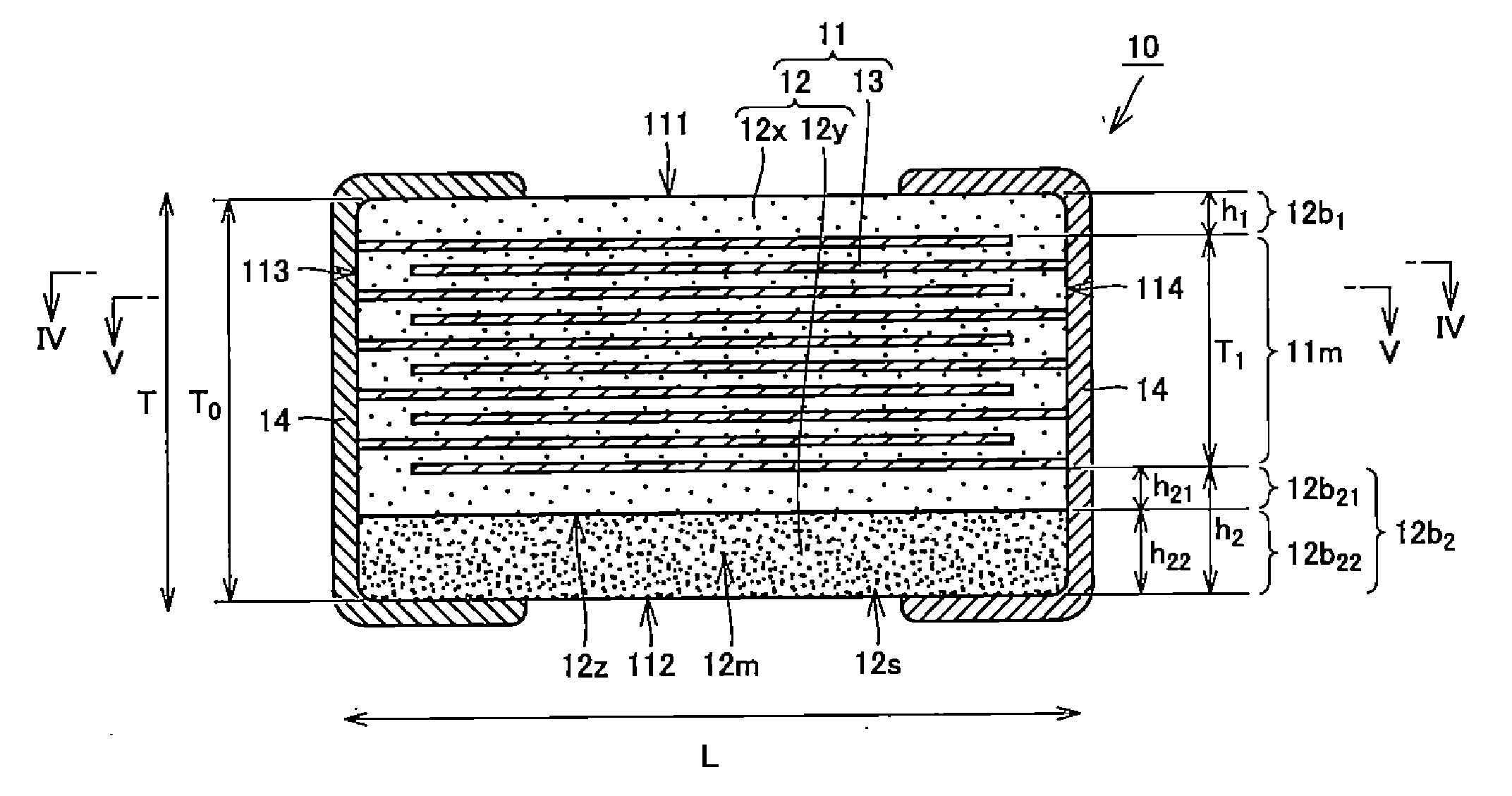
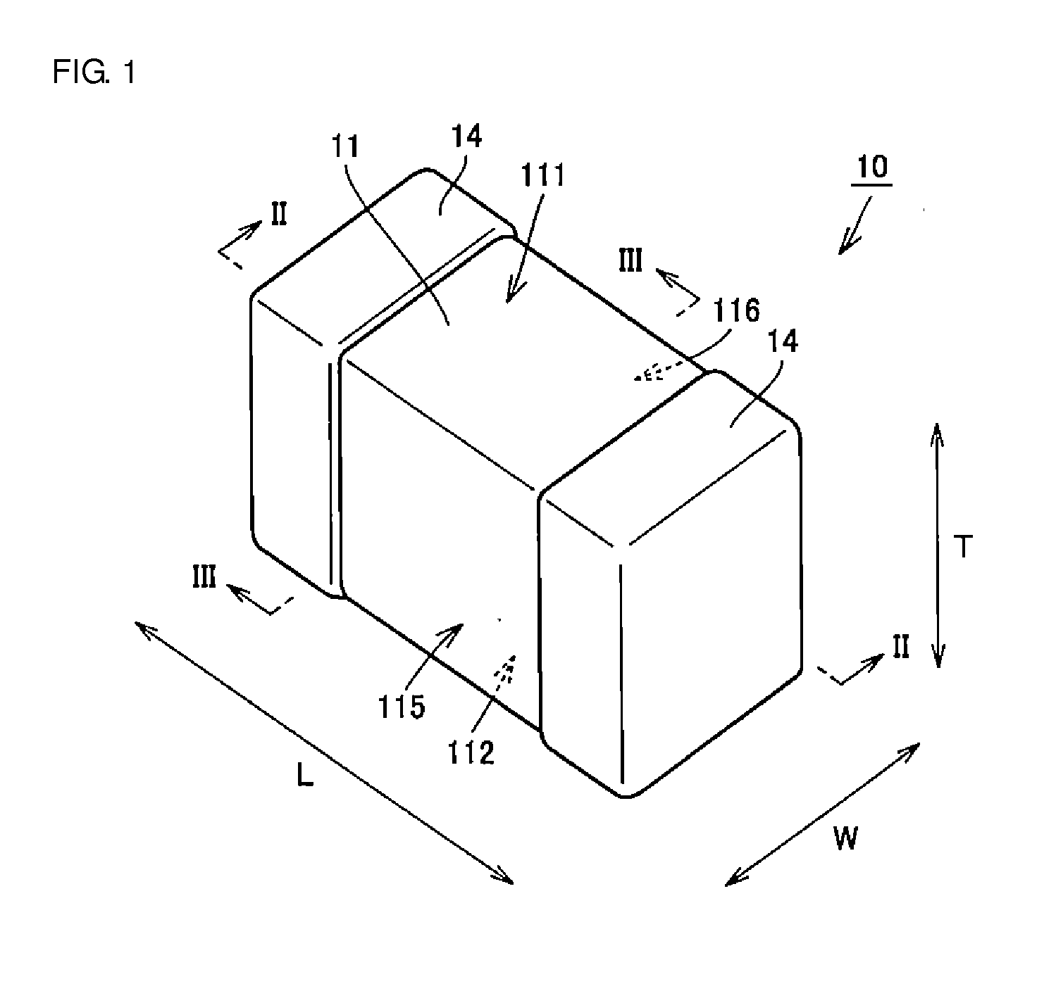
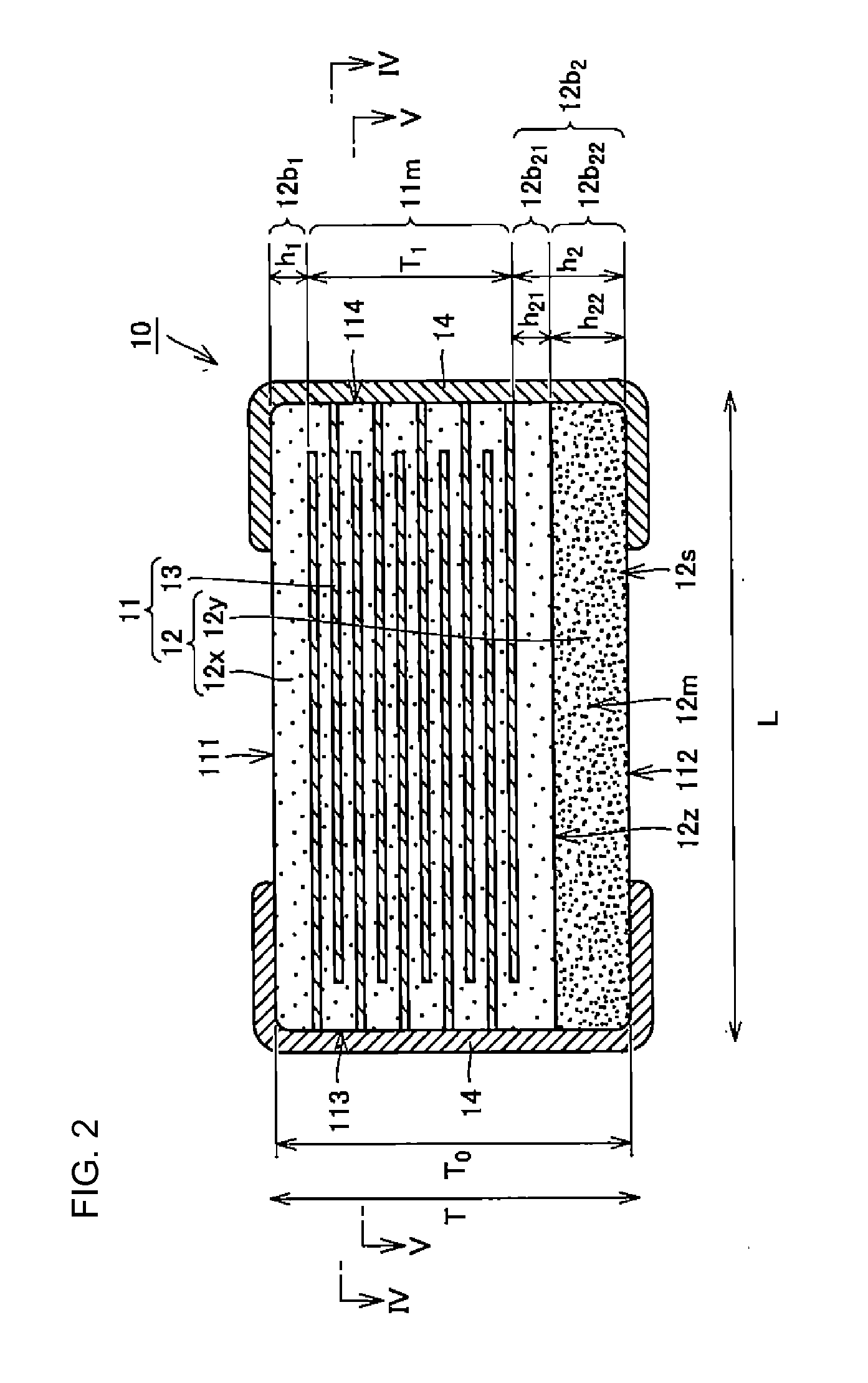
[0043]FIG. 1 is a perspective view illustrating an exterior of a multilayer ceramic capacitor according to the preferred embodiment 1 of the present invention. FIG. 2 is a cross sectional view of the multilayer ceramic capacitor of FIG. 1 viewed from a line II-II arrow direction. FIG. 3 is a cross sectional view of the multilayer ceramic capacitor of FIG. 1 viewed from a line III-III arrow direction. FIG. 4 is a cross sectional view of the multilayer ceramic capacitor of FIG. 2 viewed from a line IV-IV arrow direction. FIG. 5 is a cross sectional view of the multilayer ceramic capacitor of FIG. 2 viewed from a line V-V arrow direction. In FIGS. 1 to 5, L denotes a lengthwise direction of a multilayer body which will be described below, W denotes a widthwise direction of the multilayer body, and T denotes a thickness direction of the multilayer body.
[0044]As illustrated in FIGS. 1 to 5, a multilayer ceramic capacitor 10 according to the preferred embodiment 1 of...
embodiment 2
Preferred Embodiment 2
[0137]The shape of a boundary portion between an outer portion and an inner portion of multilayer body of the multilayer ceramic capacitor according to the preferred embodiment 2 of the present invention is a shape rendered by a mother sheet group pressure-bonding method. Thus, first, the mother sheet group pressure-bonding method according to the present preferred embodiment is described.
[0138]FIG. 13 is a cross sectional view illustrating a state where mother sheet groups of the multilayer ceramic capacitors according to the preferred embodiment 2 of the present invention are being pressure-bonded. FIG. 13 illustrates the same cross sectional view as in FIG. 8. FIG. 13 illustrates only a portion that corresponds to two of partial multilayer bodies 11p.
[0139]As illustrated in FIG. 13, in the present preferred embodiment, a plurality of mother sheets defining a first outer layer portion 12b1, a plurality of mother sheets defining an inner layer portion 11m, an...
exemplary experiment 1
[0149]In the exemplary experiment 1, 21 types of multilayer ceramic capacitors, namely, comparison examples 1 to 11 and preferred embodiment examples 1 to 10 are prepared. First, conditions (design values) common for the 21 types of multilayer ceramic capacitors are described.
[0150]The thickness of the first outer layer portion is set to 40 μm, the thickness of the second outer layer portion is set to 100 μm, the thickness of the inner layer portion is set to 620 μm, the thickness of the conductive layer is set to 0.8 μm, the number of layers in the conductive layers is set to 330, and the molar ratio of Si relative to Ti in the materials of the first dielectric layer is set to 0.013.
[0151]For each one of the 21 types of multilayer ceramic capacitors including the comparison examples 1 to 11 and the preferred embodiment examples 1 to 10, the molar ratio of Si relative to Ti in the materials of the second dielectric layers of the outer portion, the thickness of the inner portion, and...
PUM
| Property | Measurement | Unit |
|---|---|---|
| Ratio | aaaaa | aaaaa |
| Dimension | aaaaa | aaaaa |
| Content | aaaaa | aaaaa |
Abstract
Description
Claims
Application Information


