Multilayer ceramic capacitor

a ceramic capacitor and multi-layer technology, applied in the direction of fixed capacitors, stacked capacitors, fixed capacitor details, etc., can solve the problems of cracks and cracks (delamination), and achieve the effect of reducing or preventing cracks

Active Publication Date: 2017-05-23
MURATA MFG CO LTD
View PDF24 Cites 3 Cited by
  • Summary
  • Abstract
  • Description
  • Claims
  • Application Information

AI Technical Summary

Benefits of technology

[0007]Preferred embodiments of the present invention provide a multilayer ceramic capacitor in which it is possible to significantly reduce or prevent the occurrence of cracks caused by an internal stress produced by the difference in the coefficient of thermal contraction between dielectric layers and conductive layers.
[0009]According to preferred embodiments of the present invention, the boundary region preferably is not a simple flat surface, but has a shape such that the outer portion clamps the inner portion via deformed portions. It is thus possible to significantly reduce or prevent the occurrence of cracks caused by an internal stress produced due to the difference in the coefficient of thermal contraction between dielectric layers and conductive layers.

Problems solved by technology

This external stress acts on a dielectric layer of the multilayer ceramic capacitor, which causes the occurrence of cracks.
This internal stress acts on the boundary between the inner layer portion and the outer layer portion, thereby causing the occurrence of cracks (delamination).

Method used


Image

  • Multilayer ceramic capacitor
  • Multilayer ceramic capacitor
  • Multilayer ceramic capacitor

Examples


first preferred embodiment

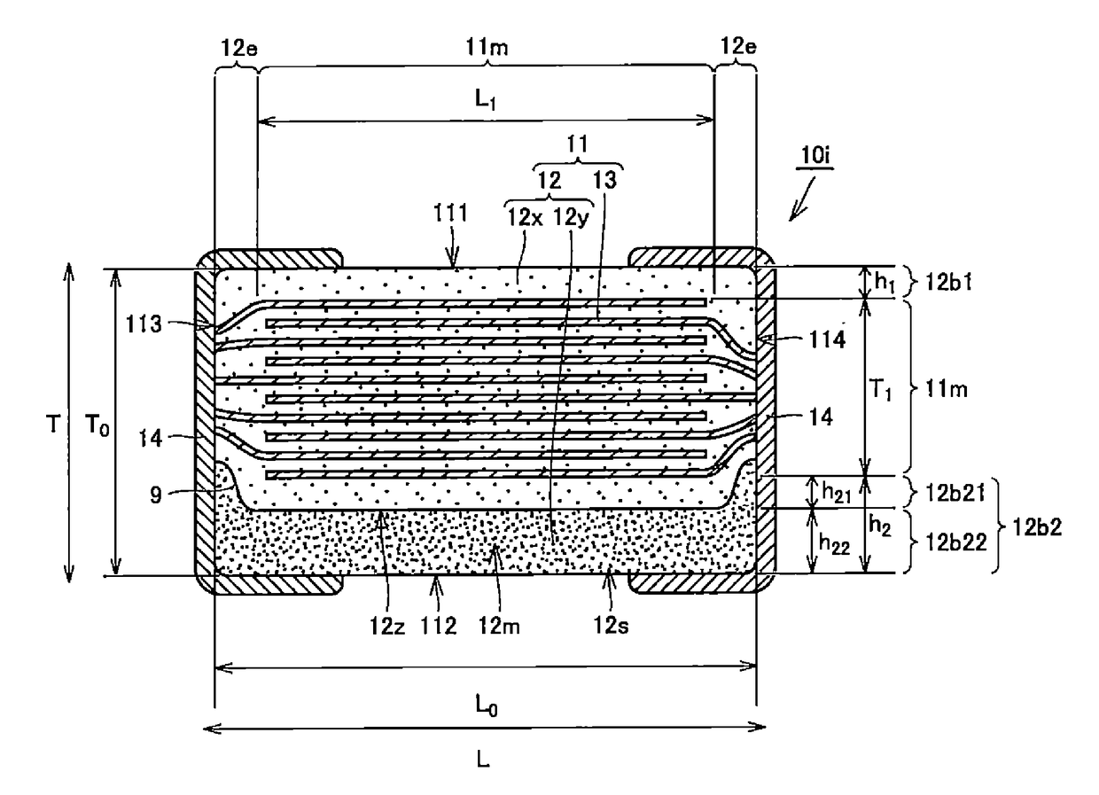
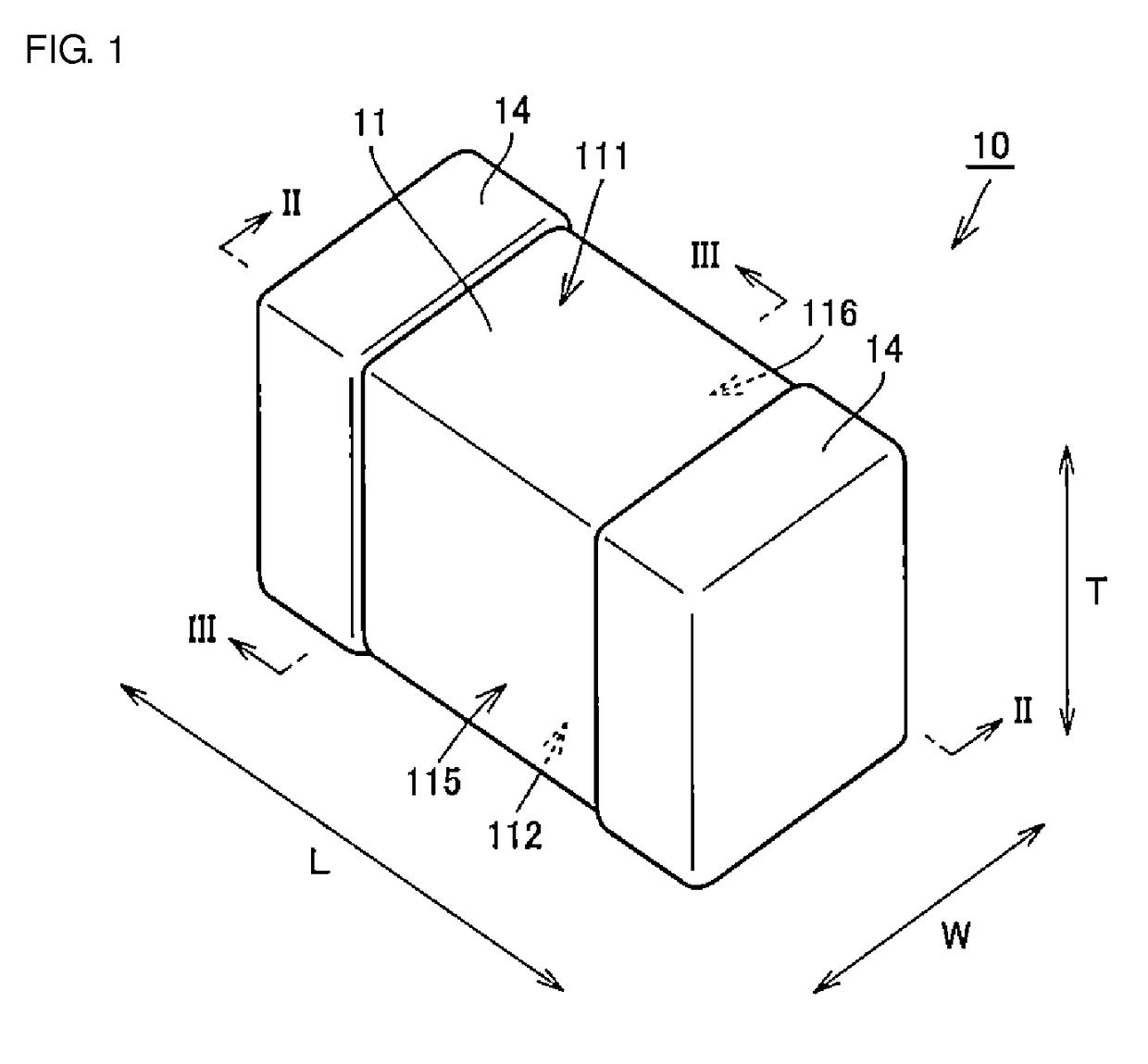
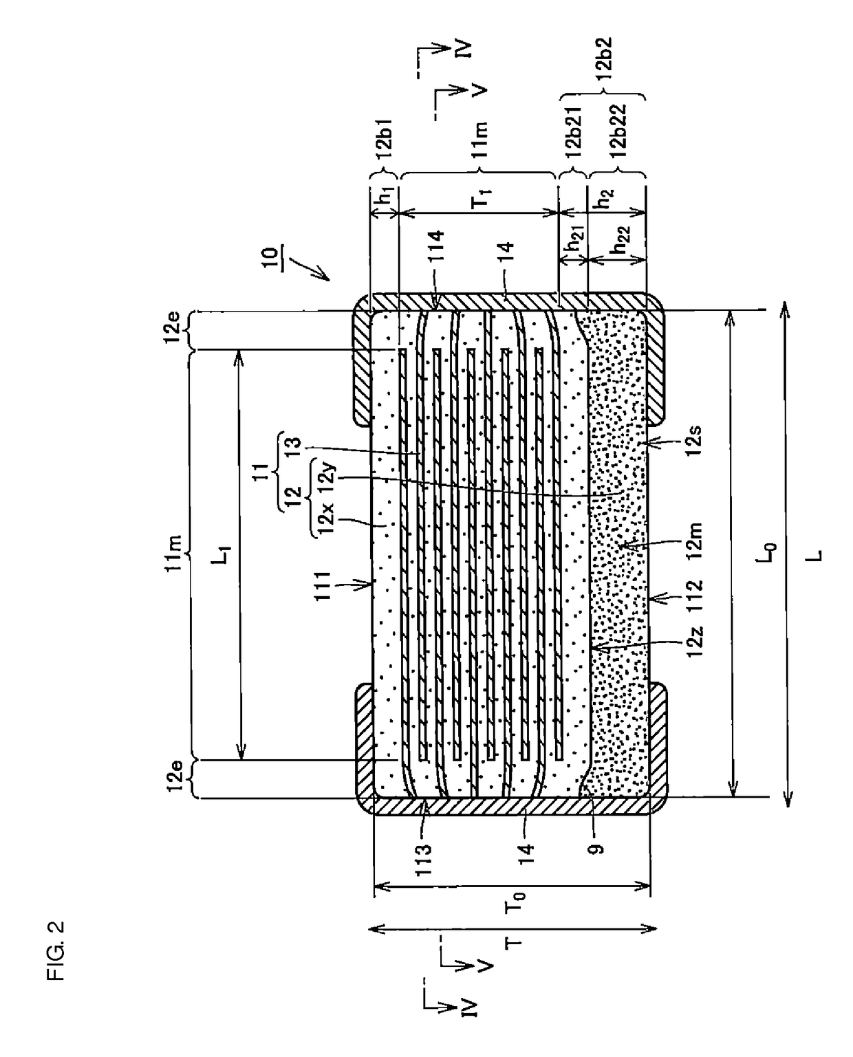
[0026]A capacitor 10 according to a first preferred embodiment of the present invention will be described below with reference to FIGS. 1 through 5.

[0027]FIG. 1 is an external perspective view of the capacitor 10. FIGS. 2 and 3 are sectional views taken along lines II-II and III-III, respectively, of FIG. 1. FIGS. 4 and 5 are sectional views taken along lines IV-IV and V-V, respectively, of FIG. 2. In FIGS. 1 through 5, the length direction of a body 11, which will be discussed below, is indicated by L, the width direction thereof is indicated by W, and the height direction thereof is indicated by T.

[0028]The stacking direction of dielectric layers 12 and conductive layers 13 is perpendicular to the length direction L and the width direction W of the body 11. That is, the stacking direction of the dielectric layers 12 and the conductive layers 13 is parallel with the height direction T of the body 11.

[0029]The capacitor 10 includes the body 11 and two outer electrodes 14. The body 1...

modified example

[0044]More preferably, instead of the capacitor 10, a capacitor 10i configured as shown in FIG. 6A is used. That is, it is preferable that, as viewed from the width direction, the points of the boundary region 12z which reach the end surfaces 113 and 114 belong to a region where the inner layer portion 11m is projected toward the end surfaces 113 and 114. That is, as shown in FIG. 6A, the positions at which both ends of the boundary region 12z are in contact with the first and second end surfaces 113 and 114 are closer to the first main surface 111 than the second outermost conductive layer 13 is. In other words, in a cross section perpendicular to a direction in which the first and second side surfaces 115 and 116 are connected to each other (in particular, a cross section passing through the center of the body 11), the distance between the points of the boundary region 12z which reach the first and second end surfaces 113 and 114 and the second main surface 112 is greater than the...

second preferred embodiment

[0066]A manufacturing method for a capacitor according to a second preferred embodiment of the present invention will be described below with reference to FIGS. 7 through 10. The manufacturing method of the second preferred embodiment is a method for manufacturing the capacitor 10 discussed in the first preferred embodiment.

[0067]FIG. 7 is a flowchart illustrating a manufacturing method for the capacitor 10 in the second preferred embodiment. In this manufacturing method, a plurality of capacitors 10 are mass-produced at one time together in the following manner. Elements which will form a plurality of capacitors 10 are processed together until a halfway point through a manufacturing process so as to fabricate a mother body. Then, the mother body is divided into individual flexible bodies. The individual flexible bodies are then processed, thus manufacturing a plurality of capacitors 10.

[0068]The manufacturing method will be discussed below more specifically with reference to FIG. 7...


PUM

PropertyMeasurementUnit
height h21aaaaaaaaaa
height h22aaaaaaaaaa
height h21aaaaaaaaaa

Abstract

A multilayer ceramic capacitor includes a body and at least two outer electrodes. The body includes first and second main surfaces, an inner layer portion and first and second outer layer portions. In the inner layer portion, dielectric layers and conductive layers are alternately stacked on each other. The second outer layer portion includes an outer portion and an inner portion. A boundary region adjacent to the inner portion in the outer portion inclines toward the first main surface.

Description

BACKGROUND OF THE INVENTION[0001]1. Field of the Invention[0002]The present invention relates to a multilayer ceramic capacitor, a multilayer ceramic capacitor series including the same, and a multilayer ceramic capacitor mount body including the same.[0003]2. Description of the Related Art[0004]An example of the related art that discloses a multilayer ceramic capacitor in which the occurrence of cracks may be suppressed is Japanese Unexamined Patent Application Publication No. 2012-248581. In the multilayer ceramic capacitor disclosed in this publication, a base unit includes an inner electrode body (inner layer portion) and first and second dielectric bodies (outer layer portions). The inner electrode body is constituted by first inner electrodes and second inner electrodes facing each other with a dielectric member therebetween and stacked on each other. The first and second dielectric bodies sandwich the inner electrode body therebetween in the stacking direction. The first diel...

Claims


Application Information

Patent Timeline
Patent Type & Authority Patents(United States)
IPC IPC(8): H01G4/30H01G4/12H01G4/012
CPCH01G4/30H01G4/012H01G4/1218H01G4/232
Inventor SUGITA, HIROAKIKITANO, SHOTA
Owner MURATA MFG CO LTD
Why Eureka
Try Eureka