Multilayer ceramic capacitor

a ceramic capacitor and multi-layer technology, applied in the direction of fixed capacitor details, fixed capacitors, printed circuit non-printed electric components association, etc., can solve the problems of cracking, no consideration is given to suppress the occurrence of cracks caused by internal stress, etc., to reduce or prevent the occurrence of cracks

Active Publication Date: 2017-05-02
MURATA MFG CO LTD
View PDF23 Cites 5 Cited by
  • Summary
  • Abstract
  • Description
  • Claims
  • Application Information

AI Technical Summary

Benefits of technology

[0008]Accordingly, preferred embodiments of the present invention provide a multilayer ceramic capacitor capable of significantly reducing or preventing cracks caused by internal stress produced due to a difference in thermal contraction rates between the dielectric layer and the conductive layer.
[0023]Various preferred embodiments of the present invention, and modifications and combinations thereof, significantly reduce or prevent the occurrence of cracks caused by the internal stress produced due to the difference in thermal contraction rates between the dielectric layer and the conductive layer.

Problems solved by technology

In this mode, the inventors discovered that an inner stress is produced due to a difference in thermal contraction rates between the dielectric layer and the conductive layer at the time of firing of the multilayer ceramic capacitor, and this inner stress is applied to a boundary between the inner layer portion and the outer layer portion and causes a crack to occur (delamination).
In the multilayer ceramic capacitor described in Japanese Unexamined Patent Application Publication No. 2012-248581, the occurrence of cracks caused by the external stress is significantly reduced or prevented, however, no consideration is given with regard to suppression of the occurrence of cracks caused by the internal stress produced due to the difference in thermal contraction rates between the dielectric layer and the conductive layer.

Method used


Image

  • Multilayer ceramic capacitor
  • Multilayer ceramic capacitor
  • Multilayer ceramic capacitor

Examples


embodiment 1

Preferred Embodiment 1

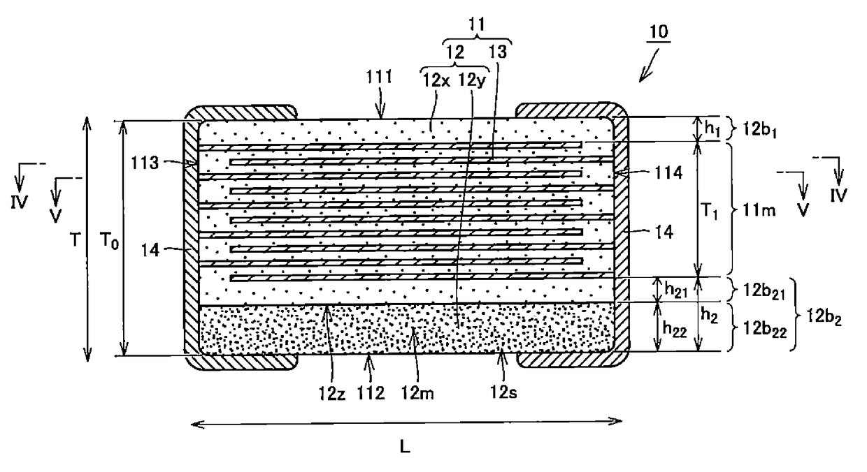
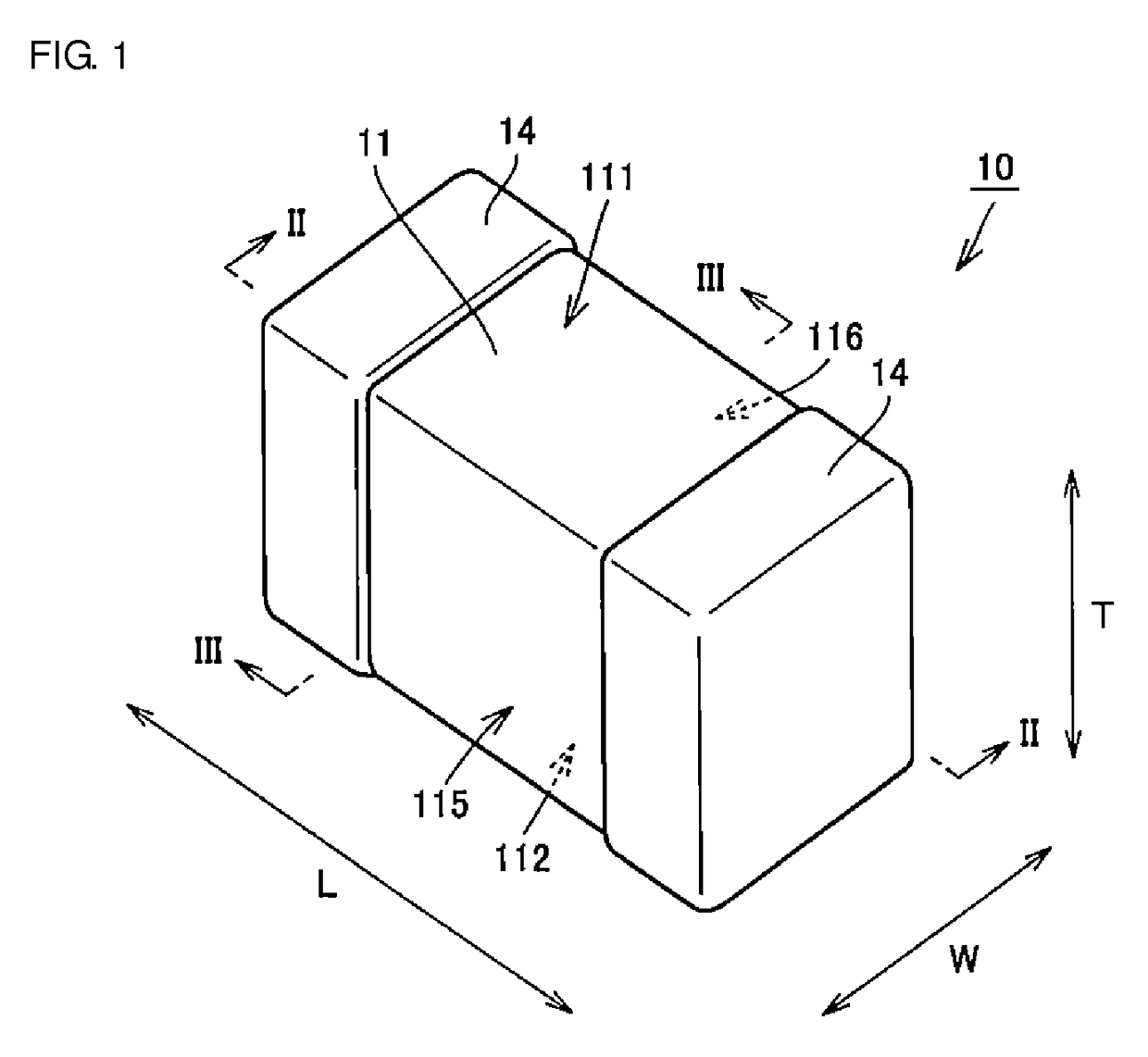
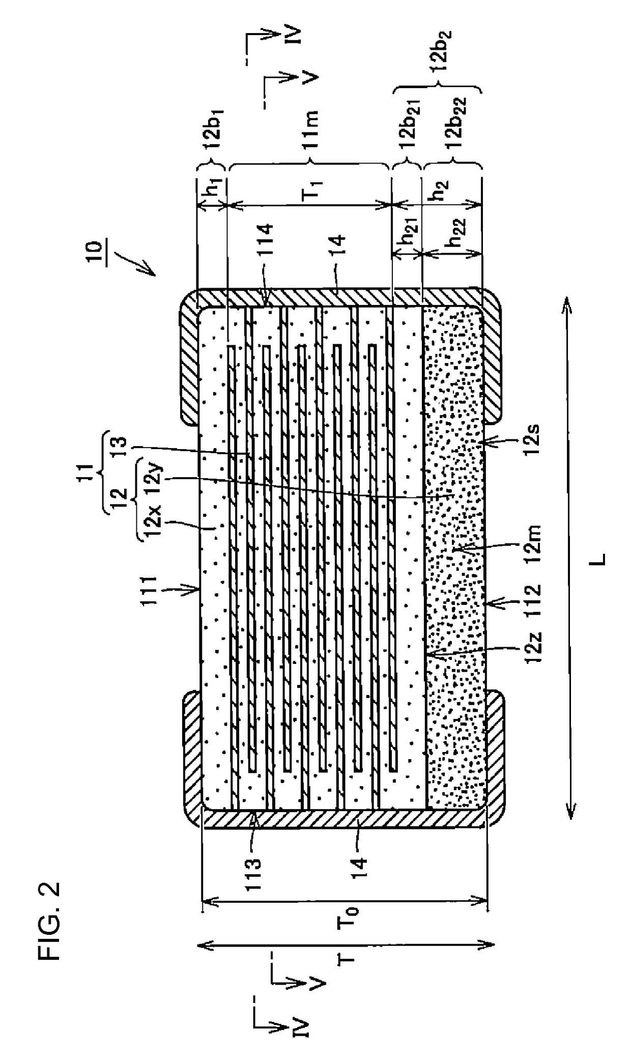
[0043]FIG. 1 is a perspective view illustrating an exterior of a multilayer ceramic capacitor according to the preferred embodiment 1 of the present invention. FIG. 2 is a cross sectional view of the multilayer ceramic capacitor of FIG. 1 viewed from a line II-II arrow direction. FIG. 3 is a cross sectional view of the multilayer ceramic capacitor of FIG. 1 viewed from a line III-III arrow direction. FIG. 4 is a cross sectional view of the multilayer ceramic capacitor of FIG. 2 viewed from a line IV-IV arrow direction. FIG. 5 is a cross sectional view of the multilayer ceramic capacitor of FIG. 2 viewed from a line V-V arrow direction. In FIGS. 1 to 5, L denotes a lengthwise direction of a multilayer body which will be described below, W denotes a widthwise direction of the multilayer body, and T denotes a thickness direction of the multilayer body.

[0044]As illustrated in FIGS. 1 to 5, a multilayer ceramic capacitor 10 according to the preferred embodiment 1 of...

embodiment 2

Preferred Embodiment 2

[0137]The shape of a boundary portion between an outer portion and an inner portion of multilayer body of the multilayer ceramic capacitor according to the preferred embodiment 2 of the present invention is a shape rendered by a mother sheet group pressure-bonding method. Thus, first, the mother sheet group pressure-bonding method according to the present preferred embodiment is described.

[0138]FIG. 13 is a cross sectional view illustrating a state where mother sheet groups of the multilayer ceramic capacitors according to the preferred embodiment 2 of the present invention are being pressure-bonded. FIG. 13 illustrates the same cross sectional view as in FIG. 8. FIG. 13 illustrates only a portion that corresponds to two of partial multilayer bodies 11p.

[0139]As illustrated in FIG. 13, in the present preferred embodiment, a plurality of mother sheets defining a first outer layer portion 12b1, a plurality of mother sheets defining an inner layer portion 11m, an...

exemplary experiment 1

[0149]In the exemplary experiment 1, 21 types of multilayer ceramic capacitors, namely, comparison examples 1 to 11 and preferred embodiment examples 1 to 10 are prepared. First, conditions (design values) common for the 21 types of multilayer ceramic capacitors are described.

[0150]The thickness of the first outer layer portion is set to 40 μm, the thickness of the second outer layer portion is set to 100 μm, the thickness of the inner layer portion is set to 620 μm, the thickness of the conductive layer is set to 0.8 μm, the number of layers in the conductive layers is set to 330, and the molar ratio of Si relative to Ti in the materials of the first dielectric layer is set to 0.013.

[0151]For each one of the 21 types of multilayer ceramic capacitors including the comparison examples 1 to 11 and the preferred embodiment examples 1 to 10, the molar ratio of Si relative to Ti in the materials of the second dielectric layers of the outer portion, the thickness of the inner portion, and...


PUM

PropertyMeasurementUnit
thickness h22aaaaaaaaaa
thickness h21aaaaaaaaaa

Abstract

A multilayer body includes an inner layer portion having a dimension in a stacking direction greater than a dimension of the inner layer portion in a width direction, a second outer layer portion including an outer portion including a second principle surface and an inner portion disposed adjacent to both of the outer portion and the inner layer portion, a dimension of the outer portion in the stacking direction being greater than a dimension of the inner portion, and a composition ratio of Si relative to Ti in the outer portion is greater than that in the inner portion.

Description

BACKGROUND OF THE INVENTION[0001]1. Field of the Invention[0002]The present invention relates to multilayer ceramic capacitors, multilayer ceramic capacitor arrays, and multilayer ceramic capacitor mounted bodies.[0003]2. Description of the Related Art[0004]Japanese Unexamined Patent Application Publication No. 2012-248581 discloses a multilayer ceramic capacitor that suppresses the occurrence of cracks. In the multilayer ceramic capacitor described in Japanese Unexamined Patent Application Publication No. 2012-248581, a base body includes an inner electrode multilayer body (inner layer portion) in which a first inner electrode and a second internal electrode are stacked so as to face each other with a dielectric therebetween; and a first dielectric multilayer body (outer layer) and a second dielectric multilayer body (outer layer) that sandwich the inner electrode multilayer body (inner layer portion) from both sides thereof in a stacking direction. Further, the first dielectric mu...

Claims


Application Information

Patent Timeline
Patent Type & Authority Patents(United States)
IPC IPC(8): H01G4/30H01G4/12H01G4/232
CPCH01G4/30H01G4/1209H01G4/232H01G4/1218H01G4/228H01G4/38H05K1/18H05K2201/10015
Inventor SUGITA, HIROAKIKITANO, SHOTA
Owner MURATA MFG CO LTD
Why Eureka
Try Eureka