Photocathode and electron tube

a photocathode and electron tube technology, applied in the field of photocathodes and electron tubes, can solve the problems of not being practicable, difficult to keep lattice matching at a wavelength of 1.7 .mu.m or longer and acquire reproducibility

Inactive Publication Date: 2002-01-31
HAMAMATSU PHOTONICS KK
View PDF0 Cites 10 Cited by
  • Summary
  • Abstract
  • Description
  • Claims
  • Application Information

AI Technical Summary

Benefits of technology

[0019] Preferably, the As composition ratio x2 of the buffer layer changes stepwise or continuously from the substrate side to the light-absorbing layer side. As a consequence, lattice mismatching is alleviated between the buffer layer and the substrate and light-absorbing layer.

Problems solved by technology

However, even with these techniques, photocathodes having a favorable sensitivity in the infrared region, a region on the longer wavelength side from a wavelength of 1.7 .mu.m in particular, have not come into practice.
The technique of literature 4 is problematic in that it is hard to keep lattice matching at a wavelength of 1.7 .mu.m or longer and acquire reproducibility.
The technique of literature 5 is disadvantageous in that the light absorption among sub-bands yields a lower absorption efficiency than the light absorption among conventional band to band, or inter bands does, thereby resultantly yielding a low photoelectric conversion efficiency.

Method used


Image

  • Photocathode and electron tube
  • Photocathode and electron tube
  • Photocathode and electron tube

Examples


Embodiment Construction

made capable of detection up to a longer wavelength, and the respective modes disclosed in literatures 2 and 4 (hereinafter referred to as Conventional Examples 1 and 2, respectively).

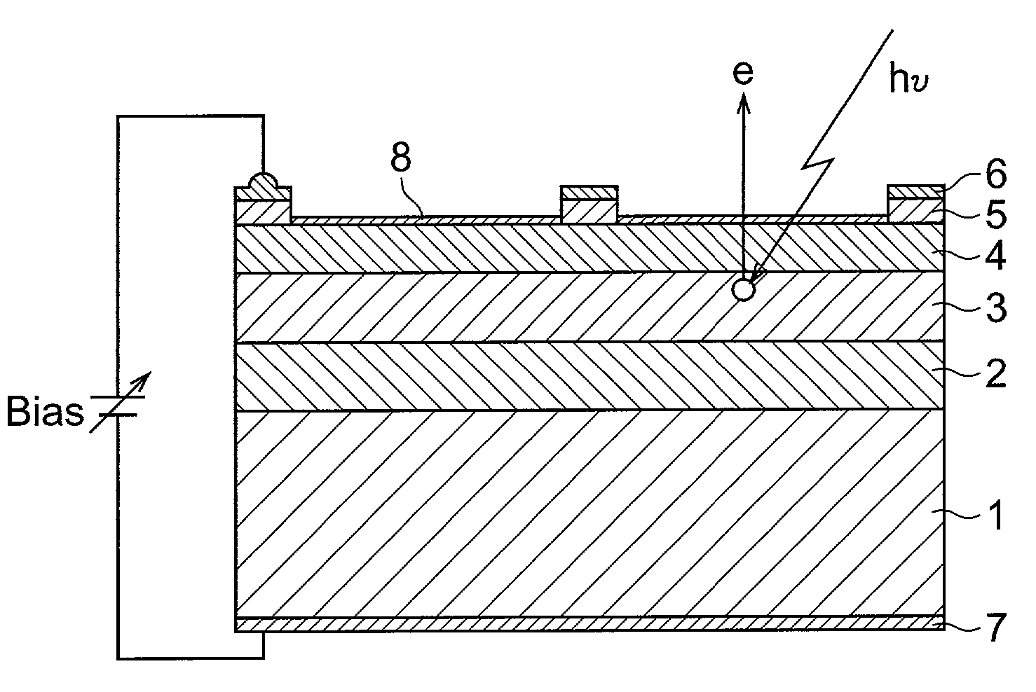
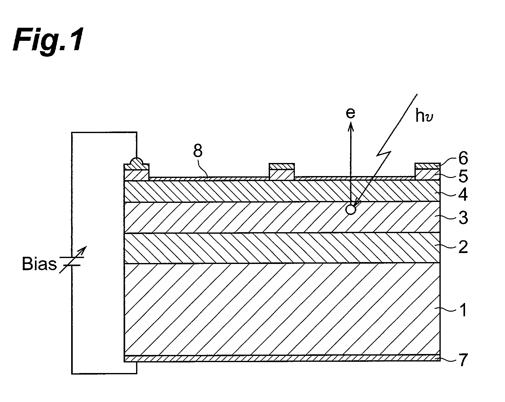
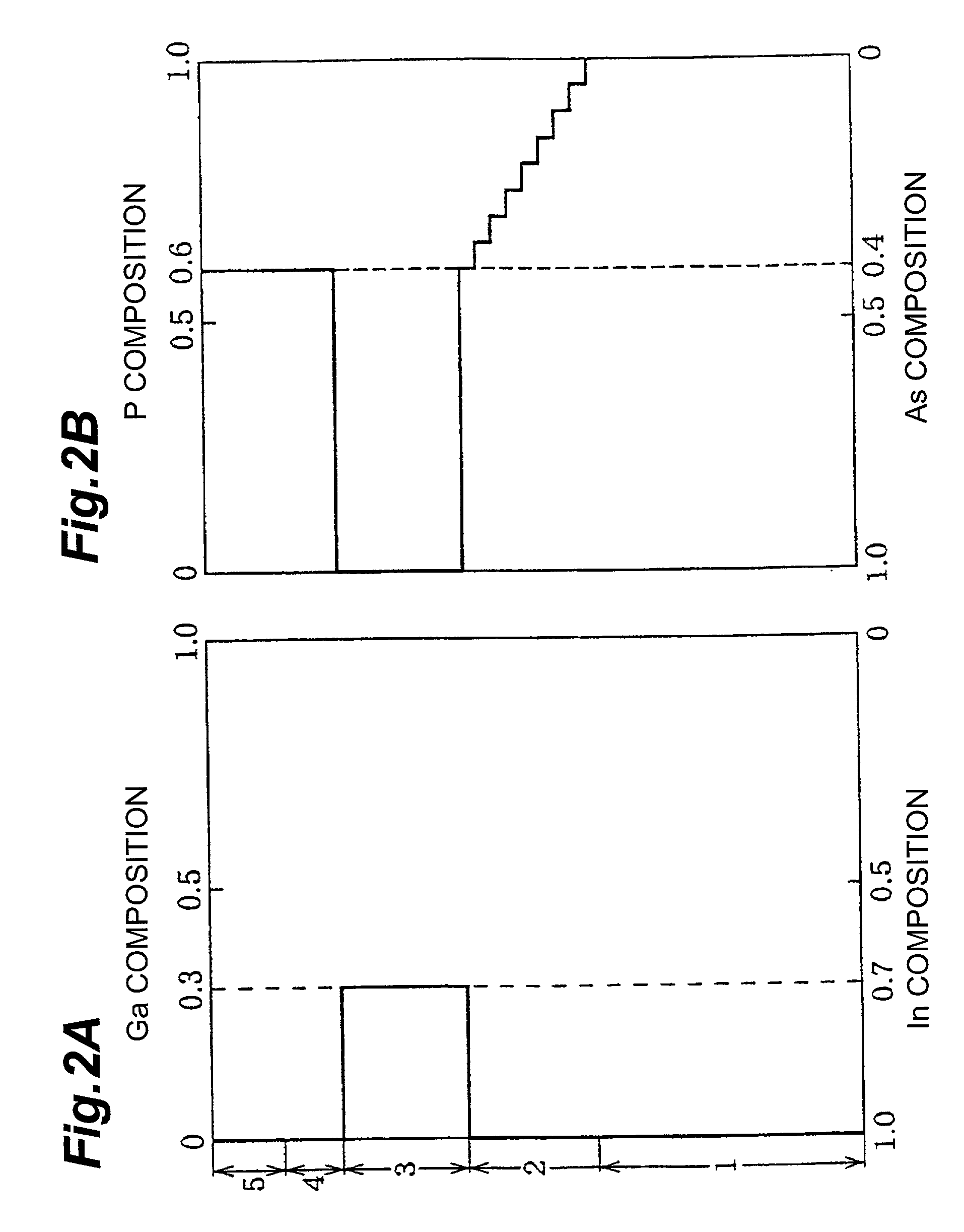
[0054] Example 2 has a basic configuration identical to that of the first embodiment shown in FIG. 1, whereas the light-absorbing layer 3 is constituted by In.sub.0.82Ga.sub.0.18As so as to be capable of detection up to a longer wavelength. In order to lattice-match the light-absorbing layer 3 at the interface, the topmost surface of buffer layer 2 has a composition of InAs.sub.0.6P.sub.0.4. Consequently, both have the same lattice constant of 5.990 angstroms as shown in FIG. 5. Similarly, the electron-emitting layer 4 and contact layer have a composition of InAs.sub.0.6P.sub.0.4, so as to yield the same lattice constant, thereby achieving lattice matching.

[0055] FIGS. 7 and 8 are graphs comparing spectral sensitivity characteristics of Examples 1 and 2 and Conventional Examples 1 and 2, whose ordinate...


PUM


Abstract

This photocathode comprises: InP substrate 1; InAsx2P1-x2(0<x2<1) buffer layer 2; Inx1Ga1-x1As (1>x1>0.53) light-absorbing layer 3; InAsx3P1-x3 (0<x3<1) electron-emitting layer 4; InAsx3P1-x3 contact layer 5 formed on the electron-emitting layer 4; active layer 8 of an alkali metal or its oxide or fluoride formed on the exposed surface of electron-emitting layer 4; and electrodes 6 and 7.

Description

[0001] This application claims priority to Provisional Application Ser. No. 60 / 220,654 filed on Jul. 25, 2000, which is hereby incorporated by reference in its entirety.[0002] 1. Field of the Invention[0003] The present invention relates to a photocathode (photoelectron-emitting surface) for emitting a photoelectron in response to a photon incident thereon, and an electron tube using the same. In particular, it relates to a photocathode for detecting light in an infrared region, and an electron tube using the same.[0004] 2. Related Background Art[0005] Concerning photocathodes which have a sensitivity in a long wavelength region among those absorbing incident light, exciting a photoelectron, and emitting it, there are techniques such as those described in U.S. Pat. No. 3,958,143 (hereinafter referred to as literature 1), Japanese Pat. Application Laid-Open No. H04-269419 (literature 2), P. E. Gregory, et al., "Field-assisted photoemission to 2.1 microns from a Ag / .rho.-In.sub.0.77Ga...

Claims


Application Information

Patent Timeline
Patent Type & Authority Applications(United States)
IPC IPC(8): H01J1/34
CPCH01J1/34H01J2201/3423
Inventor NIIGAKI, MINORUHIROHATA, TORUMOCHIZUKI, TOMOKOKAN, HIROFUMI
Owner HAMAMATSU PHOTONICS KK
Why Eureka
Try Eureka