Eureka AIR delivers breakthrough ideas for toughest innovation challenges, trusted by R&D personnel around the world.

Memory device and input signal control method of a memory device

Inactive Publication Date: 2005-05-05
SAMSUNG ELECTRONICS CO LTD
View PDF23 Cites 0 Cited by
  • Summary
  • Abstract
  • Description
  • Claims
  • Application Information

AI Technical Summary

Benefits of technology

[0013] The control unit may include a first transmission unit and a second transmission unit. In response to a control signal, the first transmission unit either connects or disconnects an input pin and a bus interface logic. In response to an inverse control signal, the second transmission unit either connects or disconnects an inverting input pin and a bus interface logic. The input pins and the address separation unit are connected. If the control signal is at a first level, the first transmission unit connects the input pin and the bus interface logic. If the inverse control signal is at a first level, the second transmission unit connects the inverting input pin and the bus interface logic. The first transmission unit and the second transmission unit may be a switch or a transmission gate. In embodiments, the control signal is a mode

Problems solved by technology

However, differential signaling technology requires twice as many I / O pins compared to single-ended signaling technology.
Due to the limited number of pins and a complex design, memory devices that use single-ended signaling technology may be limited to either a first test mode (in which data and addresses are input through one pin) or a second test mode (in which data and addresses are inputted separately).

Method used


Image

  • Memory device and input signal control method of a memory device
  • Memory device and input signal control method of a memory device
  • Memory device and input signal control method of a memory device

Examples


Embodiment Construction

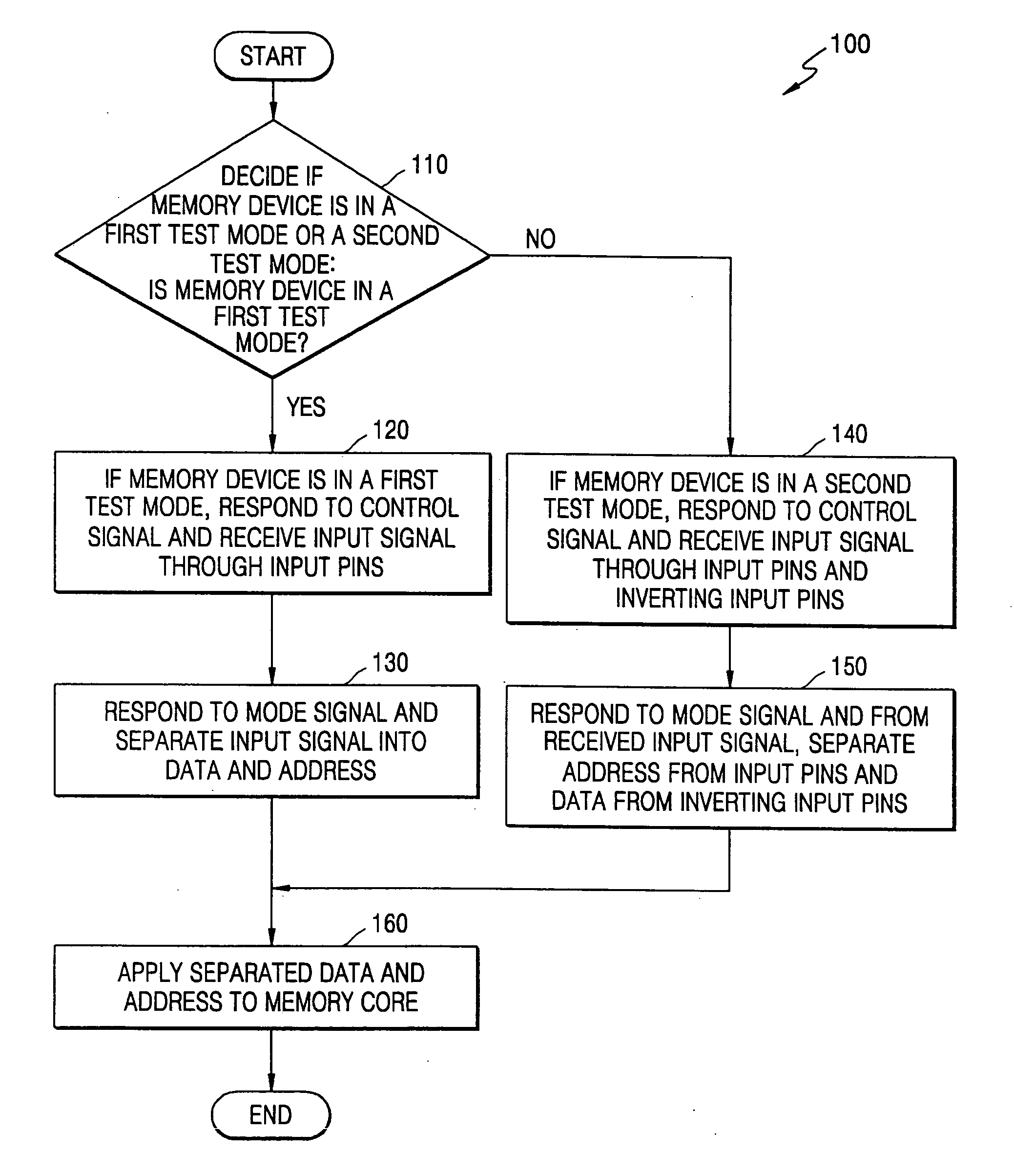
[0022] Example FIG. 1 is a flow chart illustrating a method of controlling an input signal of a memory device for each test mode, according to embodiments of the present invention. Method 100 controls input signals of a memory device for each test mode. In Step 110, it is determined whether the memory device is in a first test mode or a second test mode. In Step 120, in response to a control signal, if the memory device is in the first test mode, the input signal is received through input pins. In Step 130, in response to a mode signal, the input signal is separated into data and an address. In Step 160, the separated input signals are applied to the core of a memory device. In Step 140, if the memory device is in the second test mode, in response to a control signal, the input signal is received at input pins and inverting input pins. In Step 150, in response to a mode signal, addresses from input signals received through input pins are separated and data from the input signals rec...


PUM


Abstract

A memory device and a method of controlling an input signal of the memory device. In the method of controlling an input signal according to test modes, it is determined whether the input signal is in a first test mode or a second test mode. If the memory device is in the first test mode, in response to a control signal, an input signal is received through input pins. In response to a mode signal, the input signal is separated into data and an address. The separated data and address is applied to the core of a memory device. If the memory device is in the second test mode, an input signal is received through input pins and inverting input pins. In response to a mode signal, an address is separated from the input signal received through the input pins and the data is separated from the input signal received through the inverting input pins. The separated data and address are applied to the core of a memory device.

Description

BACKGROUND OF THE INVENTION [0001] 1. Field of the Invention [0002] Embodiments of the present invention relate to a memory device or a method of controlling input signals input into a memory device. In embodiments, separation of data and addresses from input signals is controlled. This application claims the priority of Korean Patent Application No. 2003-76215, filed on Oct. 30, 2003, in the Korean Intellectual Property Office, the disclosure of which is incorporated herein in its entirety. [0003] 2. Description of the Related Art [0004] Through the development of input / output (I / O) interface technology, a variety of I / O interface technologies have been adopted in memory devices. Such I / O interface technologies include differential signaling technology. In differential signaling technology, a pair of input signals having opposite phases are input into a memory device. [0005] Compared to single-ended signaling technology (where a reference signal and an input signal are applied to a...

Claims


Application Information

Patent Timeline
IPC IPC(8): G11C7/10G11C29/48
CPCG11C29/48G11C29/1201G11C7/10
Inventor LIM, SANG-GYUCHO, SUNG-BUM
Owner SAMSUNG ELECTRONICS CO LTD
Why Eureka
Eureka Blog
Learn More