Apparatuses and methods for cleaning a substrate

a technology of apparatus and substrate, applied in the direction of cleaning with liquids, photosensitive materials, instruments, etc., can solve the problems of foam haphazardly growing around, damage to the electronic device on the semiconductor wafer, and inoperable devices on the wafer

Inactive Publication Date: 2005-06-23
LAM RES CORP
View PDF98 Cites 53 Cited by
  • Summary
  • Abstract
  • Description
  • Claims
  • Application Information

AI Technical Summary

Benefits of technology

[0014] Other aspects and advantages of the invention will become apparent from the following detailed description, taken in conjunction with the accompanying drawings, illustrating by way of example the principles of the invention.

Problems solved by technology

For example, the process of manufacturing electronic devices on semiconductor wafers involves a complex process of depositing and removing a number of layers.
If the organic photoresist is not removed, the organic photoresist will contaminate the semiconductor wafer resulting in damage to the electronic devices on the semiconductor wafer.
Similarly, these residual particles or films may cause defects such as scratches on the wafer surface which may cause devices on the wafer to become inoperable.
The problem with applying foam 114 in an open environment is that the foam haphazardly grows around brushes 110 and cannot be directed to a particular surface area of semiconductor wafer 112.
In other words, the flow of foam 114 is difficult to control when applied in an open environment.
Furthermore, different properties of foam 114 result in different cleaning capabilities, and the properties of foam 114 are also difficult to control when applied in the open environment.
The application of foam 114 in the open environment is also wasteful as a large quantity of the foam is needed to insure a uniform distribution across the surface of semiconductor wafer 112.

Method used


Image

  • Apparatuses and methods for cleaning a substrate
  • Apparatuses and methods for cleaning a substrate
  • Apparatuses and methods for cleaning a substrate

Examples


Embodiment Construction

[0024] An invention is disclosed for apparatuses and methods for cleaning a substrate. In the following description, numerous specific details are set forth in order to provide a thorough understanding of the present invention. It will be understood, however, by one of ordinary skill in the art, that the present invention may be practiced without some or all of these specific details. In other instances, well known process operations have not been described in detail in order not to unnecessarily obscure the present invention.

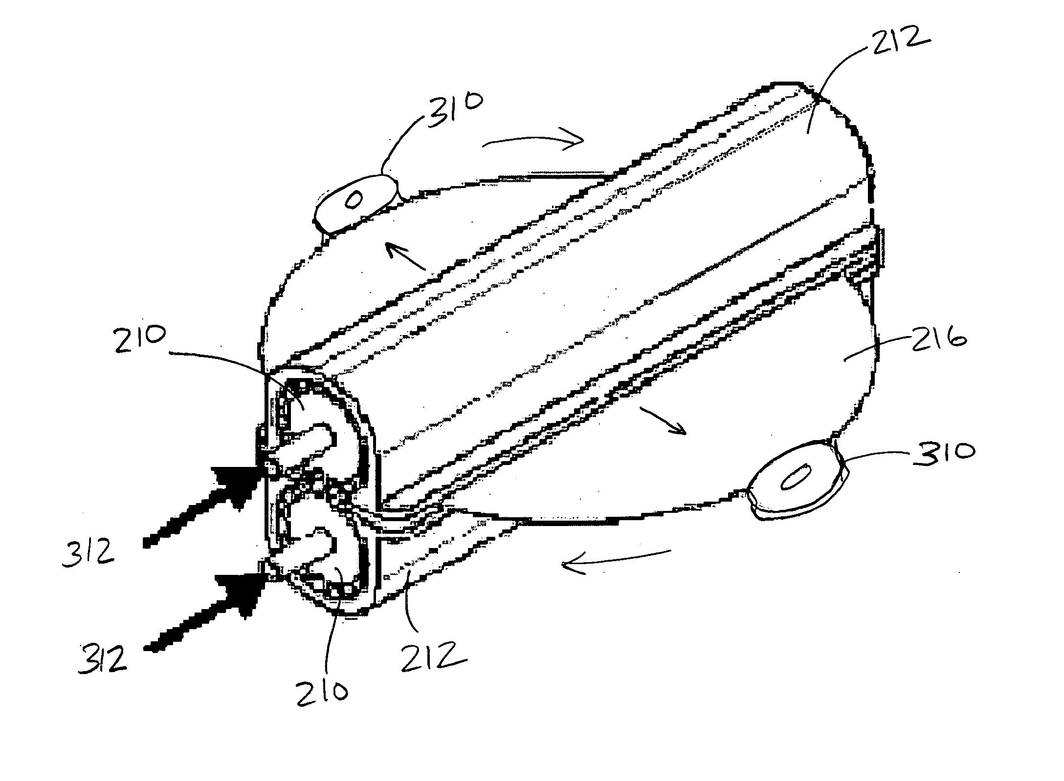
[0025] The embodiments described herein provide a brush enclosure to enclose a brush and foam. In particular, the brush enclosure is configured to contain and to control the flow and physical properties of foam. As will be explained in more detail below, the geometry of the brush enclosure creates different cleaning effects within the brush enclosure.

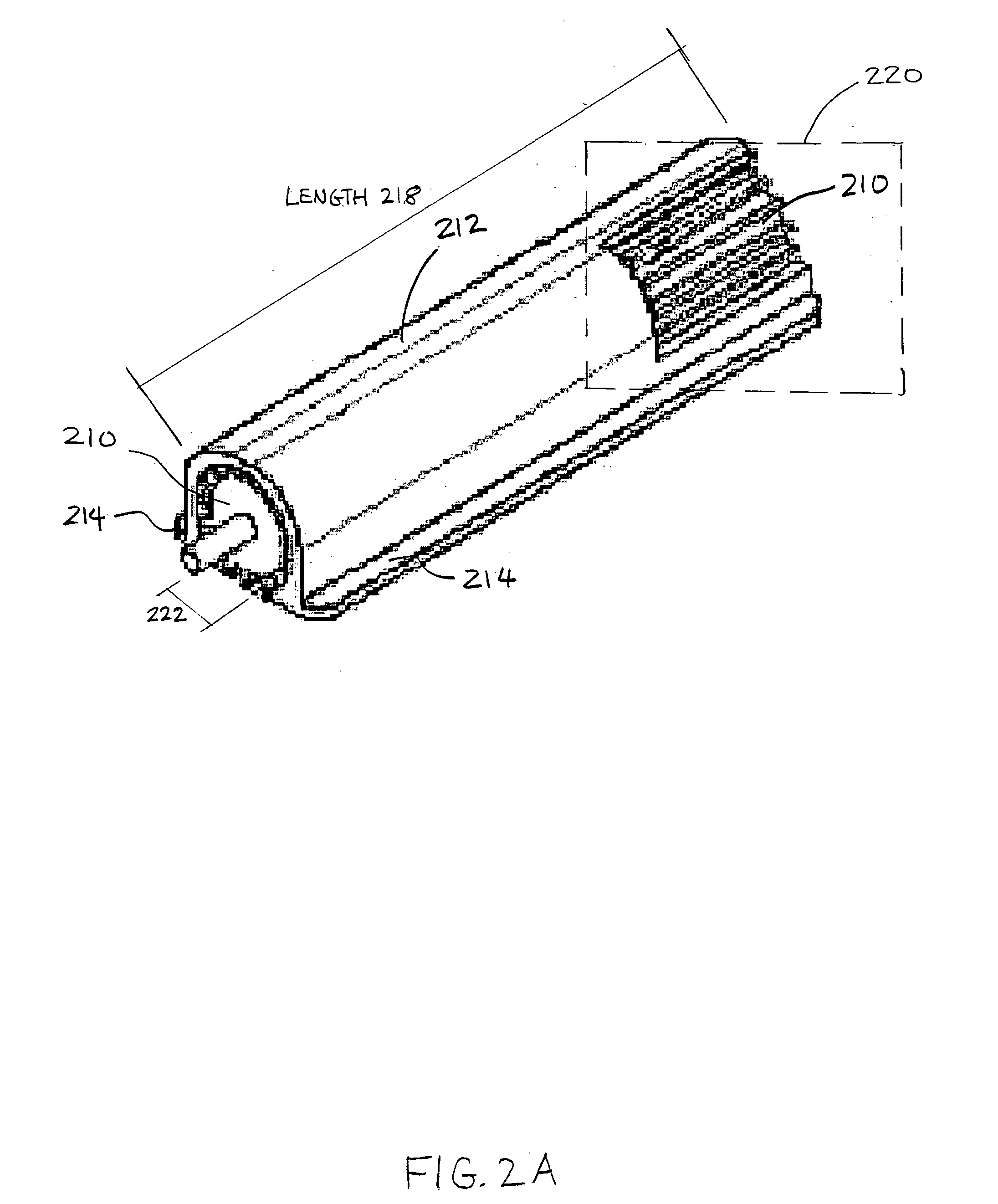
[0026]FIG. 2A is a perspective view of brush 210 partially enclosed within brush enclosure 212, in accordance ...


PUM


Abstract

An apparatus for use in processing a substrate includes a brush enclosure extending over a length. The brush enclosure is configured to be disposed over a surface of the substrate and has an open region that is configured to be disposed in proximity to the substrate. The open region extends over the length of the brush enclosure and enables foam from within the brush enclosure to contact the surface of the substrate. A substrate cleaning system and method for cleaning a substrate are also described.

Description

CROSS-REFERENCE TO RELATED APPLICATIONS [0001] This application claims priority under 35 U.S.C. § 120 as a continuation-in-part of U.S. application Ser. No. 10 / 746,114, filed Dec. 23, 2003, the disclosure of which is incorporated herein by reference. [0002] This application also relates to U.S. application Ser. No. 10 / 608,871, filed Jun. 27, 2003, the disclosure of which is incorporated herein by reference.BACKGROUND OF THE INVENTION [0003] 1. Field of the Invention [0004] The present invention relates to semiconductor manufacturing and, more particularly, to apparatuses and methods for use in processing a substrate. [0005] 2. Description of the Related Art. [0006] In the fabrication of semiconductor devices, there is a need to perform substrate (e.g., semiconductor wafer) cleaning. For example, the process of manufacturing electronic devices on semiconductor wafers involves a complex process of depositing and removing a number of layers. Typically, patterning of layer materials inc...

Claims


Application Information

Patent Timeline
Patent Type & Authority Applications(United States)
IPC IPC(8): B08B3/00H01L21/00
CPCB08B3/003Y10S134/902H01L21/67046H01L21/67028H01L21/304
Inventor DE LARIOS, JOHN M.OWCZARZ, ALEKSANDERSCHOEPP, ALANREDEKER, FRITZ
Owner LAM RES CORP
Why Eureka
Try Eureka