Tamper barrier for electronic device
- Summary
- Abstract
- Description
- Claims
- Application Information
AI Technical Summary
Benefits of technology
Problems solved by technology
Method used
Image
Examples
Embodiment Construction
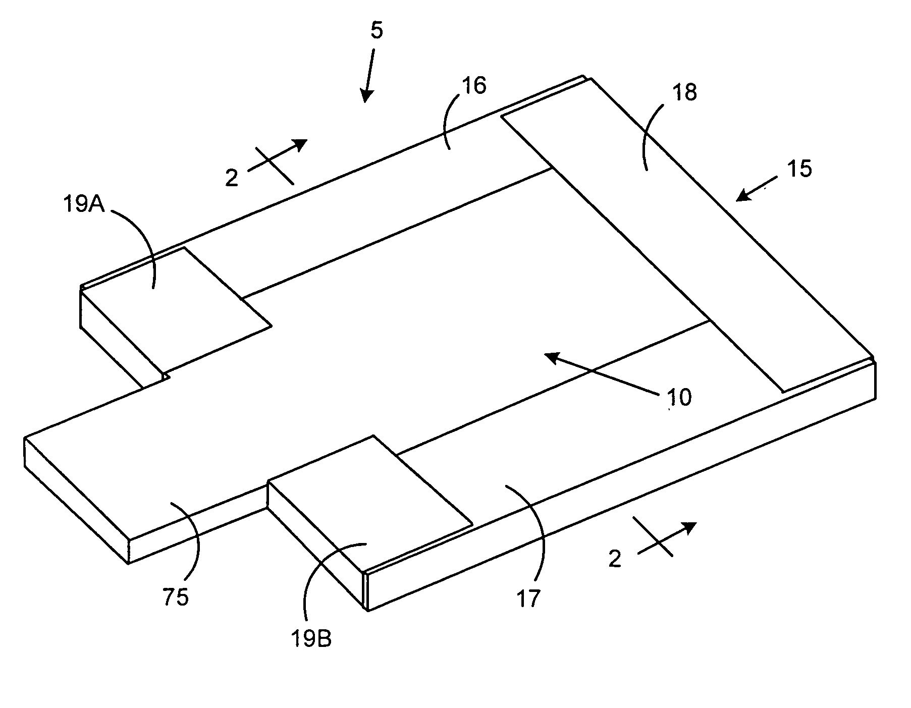
[0016] Referring to FIG. 1, the present invention relates to a PCB assembly, shown at reference numeral 5, that includes a multilayer PCB 10 and a tamper wrap 15 that partially envelops PCB 10. As described in more detail below, PCB 10 is provided with electrical security elements that provide tamper protection in the areas of PCB 10 not covered by tamper wrap 15. Together, these security elements and tamper wrap 15 provide a full envelope of tamper protection for all of the electrical components of PCB 10.
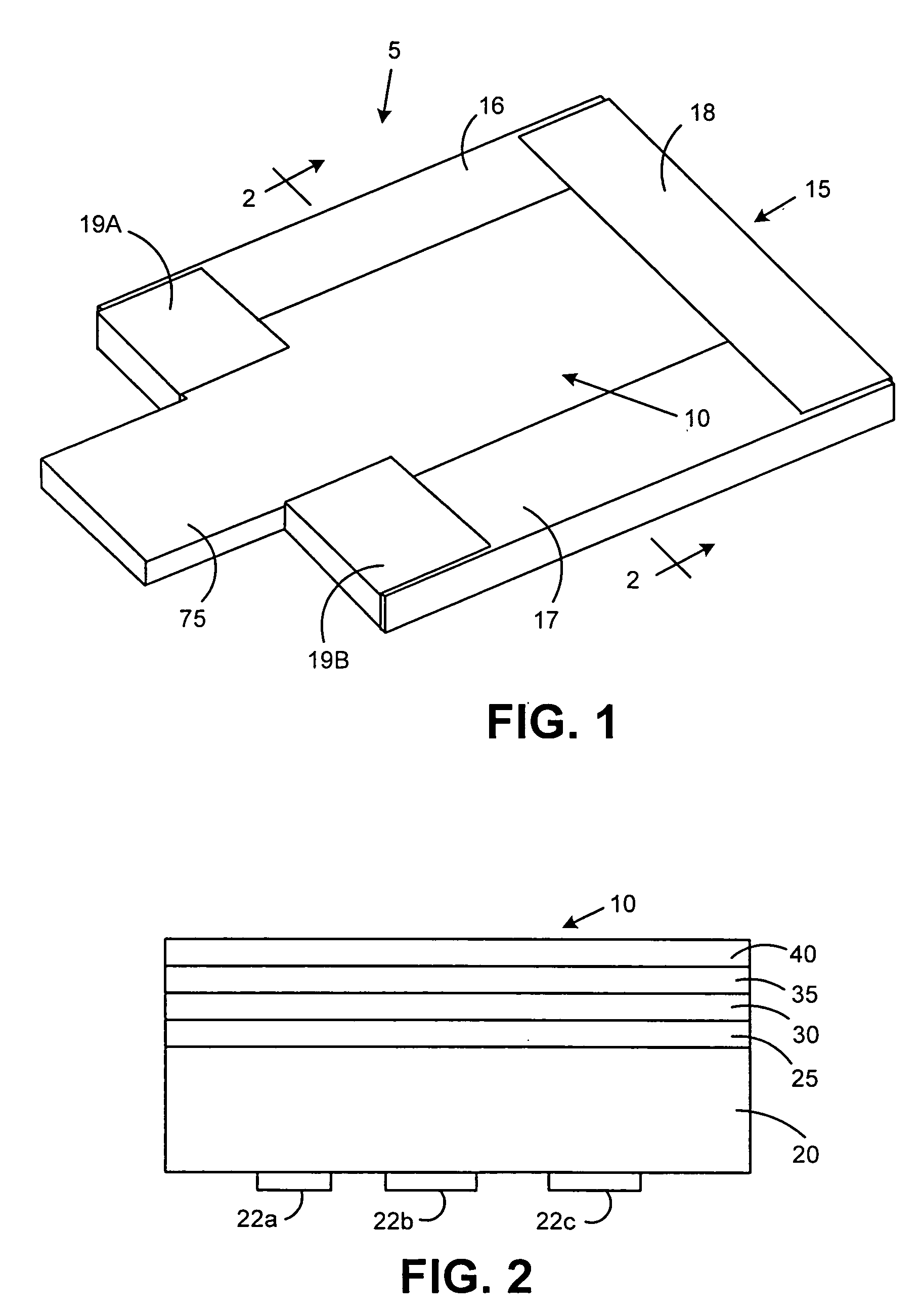
[0017] Referring to FIG. 2, a cross-sectional diagram of PCB 10 taken along lines 2-2 in FIG. 1 is provided which shows each of the layers of PCB 10. Each of the layers of PCB 10 includes a substrate or base, made of, for example, fiberglass or glass epoxy, on which various elements are provided as described herein. PCB circuitry portion 20 actually includes a number of layers, such as those included in a standard PCB, for example, a common six layer PCB. As will be appreciated b...
PUM
| Property | Measurement | Unit |
|---|---|---|
| Length | aaaaa | aaaaa |
Abstract
Description
Claims
Application Information


