Flat panel display device and method of manufacturing the same

a display device and flat panel technology, applied in the manufacture of electrode systems, tubes with screens, electric discharge tubes/lamps, etc., can solve the problems of lowering the performance of the display device, deteriorating the ability of the electrode, and deteriorating image quality, so as to reduce the uniformity of image quality, eliminate unnecessary voltage drops, and prevent the effect of increasing the resistance of the electrod

Inactive Publication Date: 2005-08-04
SAMSUNG SDI CO LTD
View PDF12 Cites 25 Cited by
  • Summary
  • Abstract
  • Description
  • Claims
  • Application Information

AI Technical Summary

Benefits of technology

[0014] An exemplary embodiment of the present invention provides a flat panel display device in which increase in electrode resistance may be prevented by forming an electrode protecting layer

Problems solved by technology

Since the variation in composition of the ITO thin film increases the inherent resistance thereof and the increase in resistance causes the voltage drop of the corresponding electrode, the abilities of the electrodes are deteriorated.
As a result, the

Method used


Image

  • Flat panel display device and method of manufacturing the same
  • Flat panel display device and method of manufacturing the same
  • Flat panel display device and method of manufacturing the same

Examples


Embodiment Construction

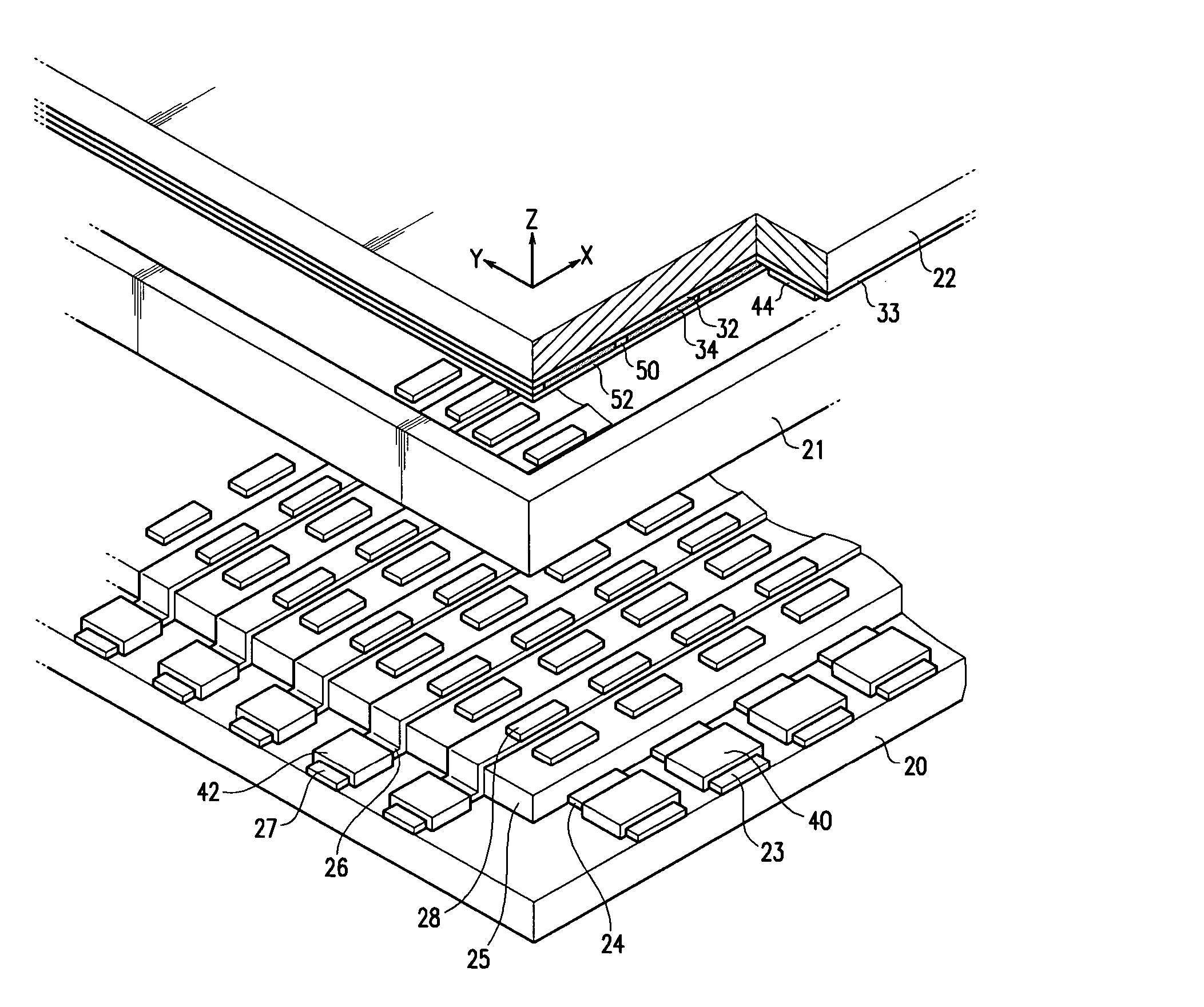
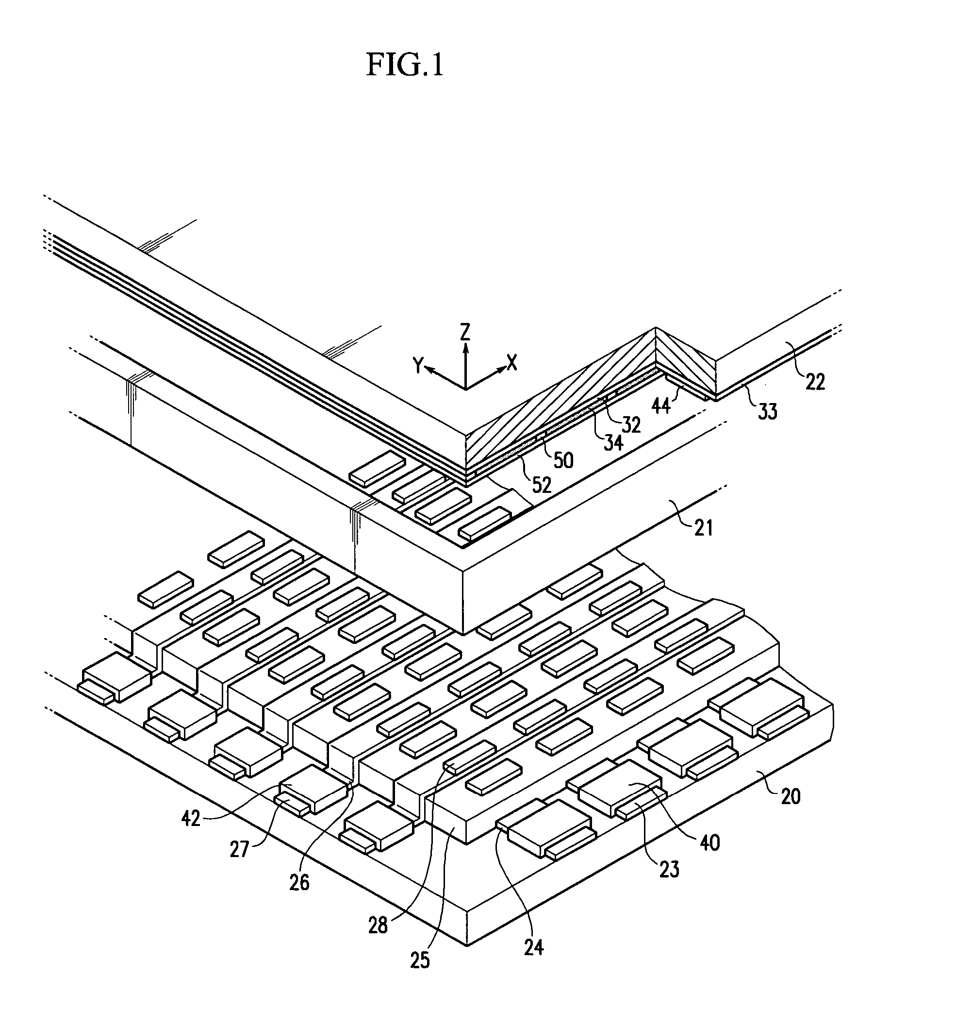
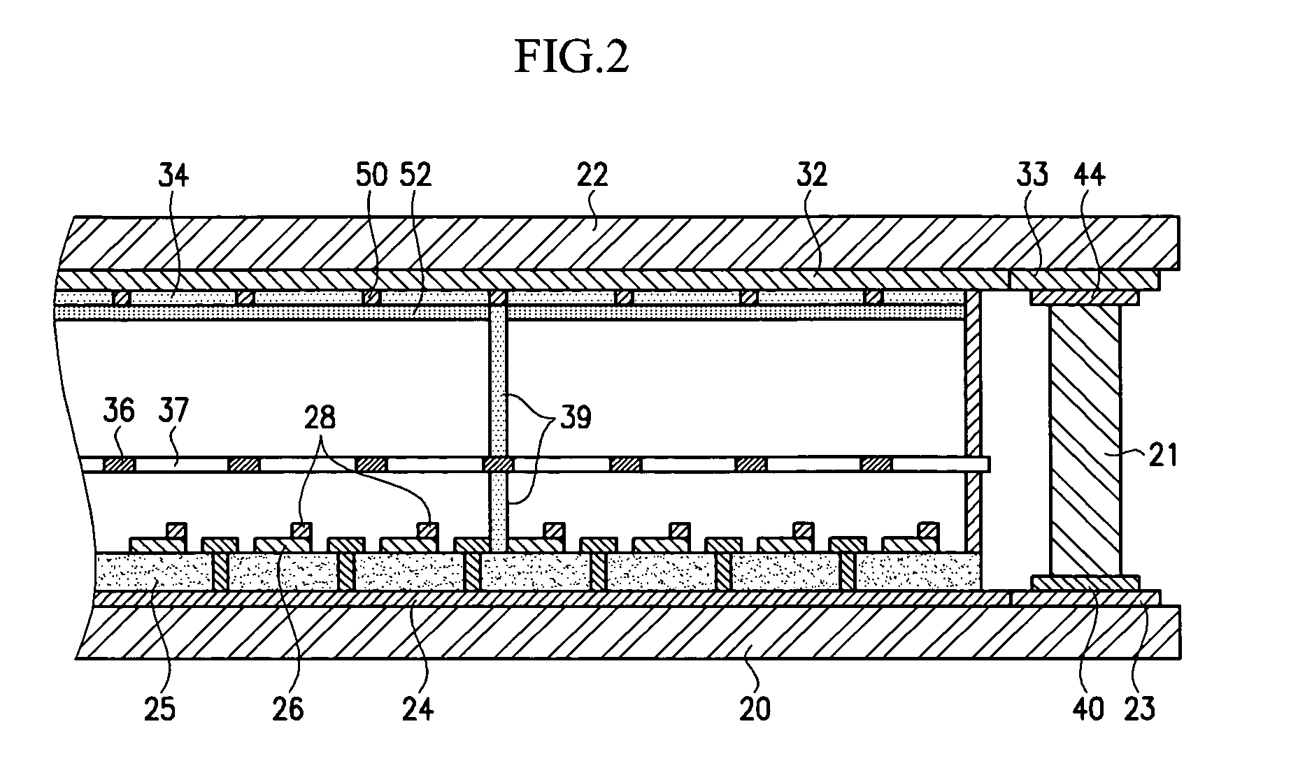
[0030] According to one embodiment of the present invention, an FEA type field emission device is shown in FIGS. 1 and 2. The field emission device includes a first substrate 20 and a second substrate 22 disposed to oppose each other with a predetermined gap therebetween. A sealing member 21 is disposed between the circumferential edges of the first substrate 20 and the second substrate 22 which seals the substrates. Gate electrodes 24 and cathode electrodes 26 are formed in a pattern intersecting each other on the first substrate 20 with an insulating layer 25 therebetween. Field emission regions 28 are formed on the portions of the cathode electrodes 26 intersecting the gate electrodes 24.

[0031] The field emission device also includes an anode electrode 32 formed on the second substrate 22 and fluorescent film 34 formed in a predetermined pattern on one surface of the anode electrode 32.

[0032] In addition, the field emission device may further include black film 50 disposed betw...


PUM


Abstract

A flat panel display device includes a first substrate and a second substrate disposed to oppose each other with a predetermined gap therebetween. An electrode made of a transparent conductive oxide film is formed on at least one of the first substrate and the second substrate. A sealing member is disposed between the first substrate and the second substrate and bonds the first substrate and the second substrate to each other. An electrode protecting layer is formed on a portion of the electrode overlapping with the sealing member and between the sealing member and the electrode.

Description

CROSS REFERENCE TO RELATED APPLICATION [0001] This application claims priority to and the benefit of Korean Patent Application No. 10-2004-0005969 filed on Jan. 30, 2004 in the Korean Intellectual Property Office, the entire content of which is incorporated herein by reference. BACKGROUND OF THE INVENTION [0002] 1. Field of the Invention [0003] The present invention relates to a flat panel display device and a method of manufacturing the flat panel display device, and more particularly, to a flat panel display device in which an increase in electrode resistance may be prevented by forming an electrode protecting layer on a portion of an electrode passing through a sealing member which also eliminates unnecessary voltage drops and prevents a decrease in brightness and decrease in uniformity of image quality, and a method of manufacturing the flat panel display device. [0004] 2. Description of the Related Art [0005] Unlike cathode ray tubes that require a large volume and a high volta...

Claims


Application Information

Patent Timeline
IPC IPC(8): G02F1/1345G09F9/00G09F9/30H01J1/05G02F1/1339H01J1/14H01J5/32H01J9/04H01J9/12H01J17/18H01J29/86H01J29/90H01J29/92H01J31/12H01L27/32H01L51/52
CPCG02F1/1345H01J5/32H01J17/18H01L51/5237H01J29/90H01L27/3281H01L51/5206H01J29/86H10K59/179H10K50/81H10K50/8426H10K50/844B23Q3/062
Inventor CHI, EUNG-JOON
Owner SAMSUNG SDI CO LTD
Why Eureka
Try Eureka