Display device

a display device and display technology, applied in the direction of static indicating devices, instruments, etc., can solve the problems of uneven emission luminance, difficult uniform control of laser irradiation intensity over the glass substrate, and difficult wiring layout, etc., to achieve efficient current transmitting circuit

Active Publication Date: 2005-08-11
RAKUTEN GRP INC
View PDF5 Cites 23 Cited by
  • Summary
  • Abstract
  • Description
  • Claims
  • Application Information

AI Technical Summary

Benefits of technology

[0055] More preferably, each of the first and second current source circuits includes a first field effect transistor having its source and drain connected to a prescribed voltage and to a first node, respectively, and its gate connected to a second node, a second field effect transistor connecting the gate and drain of the first field effect transistor in the current writing operation, and a capacitance element connected to the second node to hold source-to-drain voltage of the first field effect transistor; and each of the plurality of current transmitting circuits includes an input switch circuit connecting the corresponding second signal line to the first node of one of the first and second current source circuits that performs the current writing operation, and an output switch circuit connecting the corresponding first signal line to the first node of the other one of the first and second current source circuits that performs the current output operation.
[0056] In the display apparatus, two current source circuits alternately execute the current writing operation in which a current is written from the corresponding second signal line and the current output operation in which the current written in the current writing operation is supplied to the corresponding first signal line, and thus, an efficient current transmitting circuit can be formed.

Problems solved by technology

It is noted, however, that the low temperature p-Si TFT, which is generally formed by laser annealing, has Vth (threshold voltage) and μ (mobility) varied more widely than single-crystal silicon, because it is difficult to uniformly control laser irradiation intensity over the glass substrate.
This results in unevenness in emission luminance.
Further, it is necessary to arrange a plurality of signal lines for every column, and therefore, wiring layout becomes difficult in a display apparatus of high resolution having a narrow pixel pitch.
Therefore, when the number of bits of the image data increases together with the increase in colors to be displayed, voltage variation of an image data line transmitting the image data may possibly affects generation of the signal line driving current on a signal line supplying a current to a light emitting element.

Method used


Image

  • Display device
  • Display device
  • Display device

Examples


first embodiment

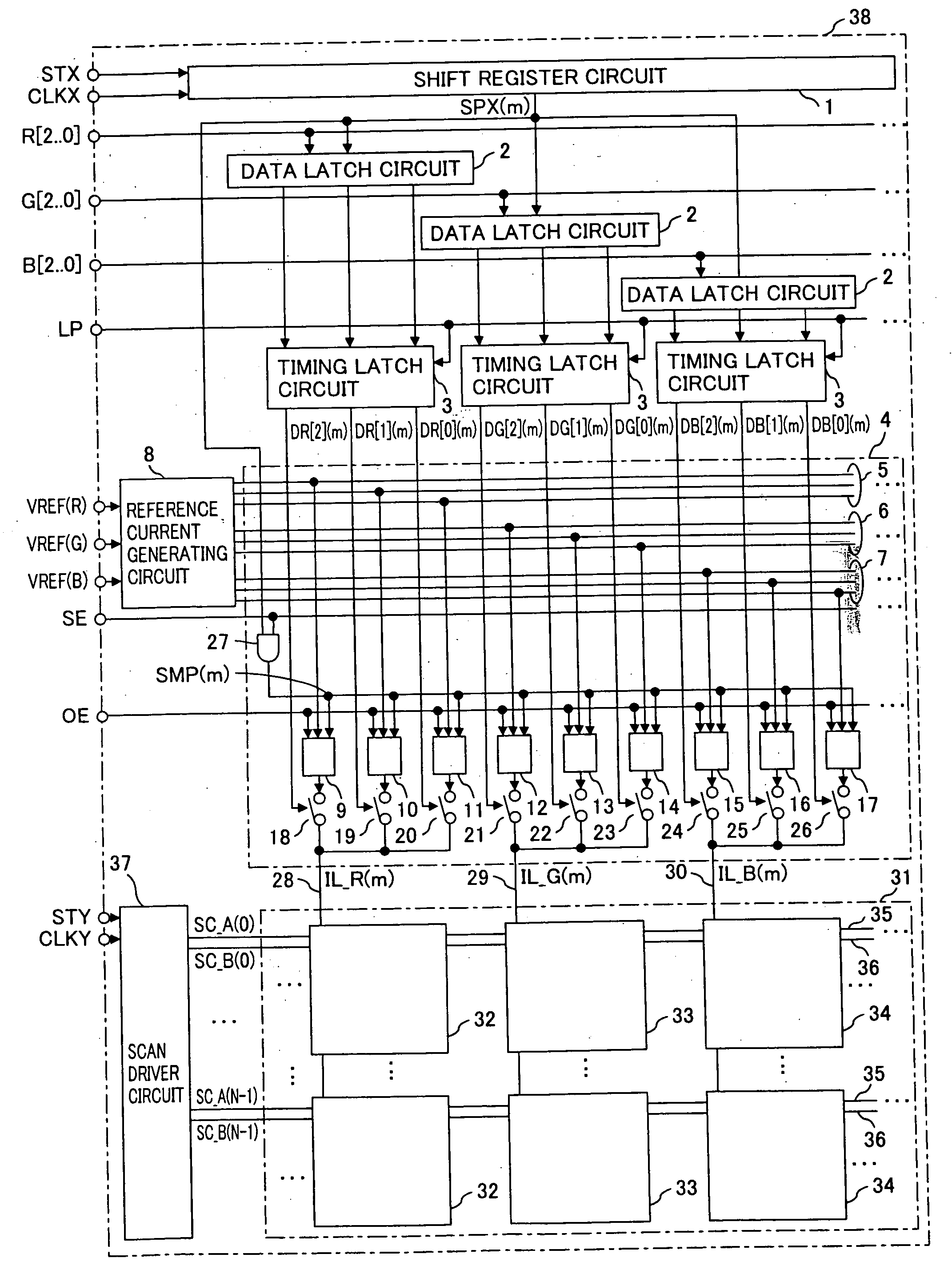
[0095]FIG. 1 is a block diagram representing a configuration of the display apparatus in accordance with a first embodiment. Here, an example will be described in which 512 colors are displayed by image data of 3-bits each for R (red), G (green) and B (Blue). The figure shows a configuration of one column (m-th column) of each of R, G and B, and the suffix m represents that the component corresponds to m-th RGB column (set of RGB columns) from the left.

[0096] Referring to FIG. 1, an organic EL panel 38 shown as a representative example of a display apparatus in accordance with the first embodiment includes a shift register circuit 1, data latch circuits 2, timing latch circuits 3, a signal line driving circuit 4, a reference current generating circuit 8, a pixel matrix 31 and a scan driver circuit 37.

[0097] Data latch circuits 2 latch input image data R[2..0], G[2..0] and B[2..0] in response to a shift pulse output from shift register circuit 1. Timing latch circuits 3 latch the i...

second embodiment

[0163]FIG. 7 is a block diagram representing a configuration of a display apparatus in accordance with a second embodiment of the present invention.

[0164] In the second embodiment, two bit weighting current source systems (system A / system B) are provided, and the operation of writing reference current and the operation of outputting the bit weighting current are performed in a complementary manner.

[0165] Referring to FIG. 7, in the second embodiment, a signal line driving circuit 4 includes, in place of bit weighting current source circuits 9 to 17 shown in FIG. 1, bit weighting current source circuits 100 to 108, each including two systems (system A / system B) of current sources. Bit weighting current source circuits 100 to 102 for R are provided in place of bit weighting current source circuits 9 to 11 for R shown in FIG. 1, bit weighting current source circuits 103 to 105 for G are provided in place of bit weighting current source circuits 12 to 14 for G shown in FIG. 1, and bit...

third embodiment

[0199] In the configurations of the first and second embodiments, the reference current is generated from the original current, using a current mirror circuit. In the third embodiment, a configuration will be described in which the original current is provided as a staircase wave current having steps corresponding to the number of bits, the current of each step is sampled and separated by reference current generating circuit 8, and the result is output as the reference current to the reference current line.

[0200]FIG. 11 is a circuit diagram representing configurations of reference current generating circuit 8 and an external circuit for generating a reference current, in accordance with the third embodiment of the present invention.

[0201] According to the third embodiment, the bit weighting reference currents IREF(R)[2] to IREF(R)[0] for R, by way of example, are generated in the following manner. A D / A converting circuit (DAC) 70 provided outside the organic EL panel is controlle...


PUM


Abstract

Signal lines for supplying signal currents to respective pixel circuits having light emitting elements are arranged. A signal line driving circuit generates, on a signal line, a signal current corresponding to the image data, by switching bit weighting currents output from bit weighting current source circuits provided for respective bits of the image data, using a switch circuit turned on/off dependent on the corresponding bit. Each current source circuit has a function of correcting the level of the bit weighting current output from itself, based on a reference current of the bit weighting current supplied from a reference current line. Therefore, even when the characteristics of TFTs forming respective current source circuits vary widely, variation in signal currents among the signal lines can be suppressed, and unevenness in emission luminance can be suppressed.

Description

TECHNICAL FIELD [0001] The present invention relates to a display apparatus including, for each pixel, a light emitting element of which emission luminance changes in accordance with a current, such as an organic EL (Electro-Luminescence) element. BACKGROUND ART [0002] Recently, display apparatus using organic ELs and the like as light emitting elements have been actively developed for portable information terminals or for television receivers. A self-emissive display apparatus including, for each pixel, a light emitting element such as an organic EL has good visibility and superior motion-image display characteristic. [0003] An example of a conventional display apparatus using the organic ELs as light emitting elements is known, by way of example, from Japanese Patent Laying-Open No. 11-212493. [0004]FIG. 37 is a circuit diagram representing a configuration of the conventional display apparatus described in the afore-mentioned laid-open application, in which four signal lines (Sm, ...

Claims


Application Information

Patent Timeline
Patent Type & Authority Applications(United States)
IPC IPC(8): G09G3/32
CPCG09G3/3241G09G3/3283G09G2300/0417G09G2320/0242G09G2300/0861G09G2310/027G09G2310/0297G09G2300/0842
Inventor AGARI, MASAFUMITOKIOKA, HIDETADAHASHIDO, RYUICHIURAKABE, TAKAHIROGOTOH, SUEHIROOKABE, MASASHIINOUE, MITSUO
Owner RAKUTEN GRP INC
Why Eureka
Try Eureka