Logic-in-memory circuit using magnetoresistive element

Active Publication Date: 2005-08-11
TOHOKU UNIV
View PDF3 Cites 15 Cited by
  • Summary
  • Abstract
  • Description
  • Claims
  • Application Information

AI Technical Summary

Benefits of technology

[0026] The magnetoresistive effect network uses the fact that the resistance change of magnetoresistive elements is smaller than that of transistors to realize the particular combination of stored values and externally input values that minimizes the resistance value of the network with less number of magnetoresistive elements and transistors.
[0027] It is desirable for the magnetoresistive effect network to have two complementary outputs, a differential pair circuit being formed using the two outputs as current paths, and to perform the threshold value detection by comparing currents flowing through each of the current paths with each other using the differential pair circuit.
[0028] The differential pair circuit can also be a dynamic type one including two phases, one being a precharge phase where the differential pair circuit is driven by a clock signal to charge capacitors connected to the current paths, and the other being an evaluation phase where currents flowing through the magnetoresistive effect network are compared with each other using the stored charges to charge another capacitor.
[0029] The magnetoresistive elements that form the magnetoresistive effect network can als

Problems solved by technology

In integrated circuits where the performance improvement of processor elements, memories, etc. is promoted with the backdrop of rapid development i

Method used


Image

  • Logic-in-memory circuit using magnetoresistive element
  • Logic-in-memory circuit using magnetoresistive element
  • Logic-in-memory circuit using magnetoresistive element

Examples


Example

[0049] Preferred embodiments of the present invention will hereinafter be described referring to the accompanying drawings.

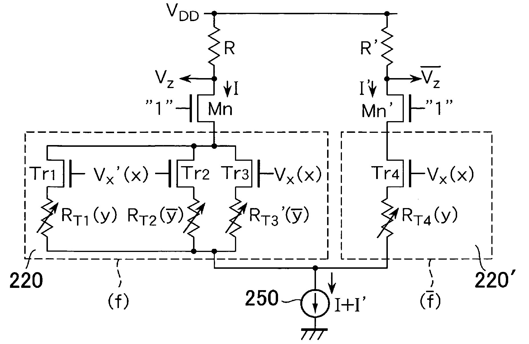
[0050]FIG. 4 is a view showing the overall configuration of a logic-in-memory circuit using TMR elements as magnetoresistive elements, i.e., variable resistive elements.

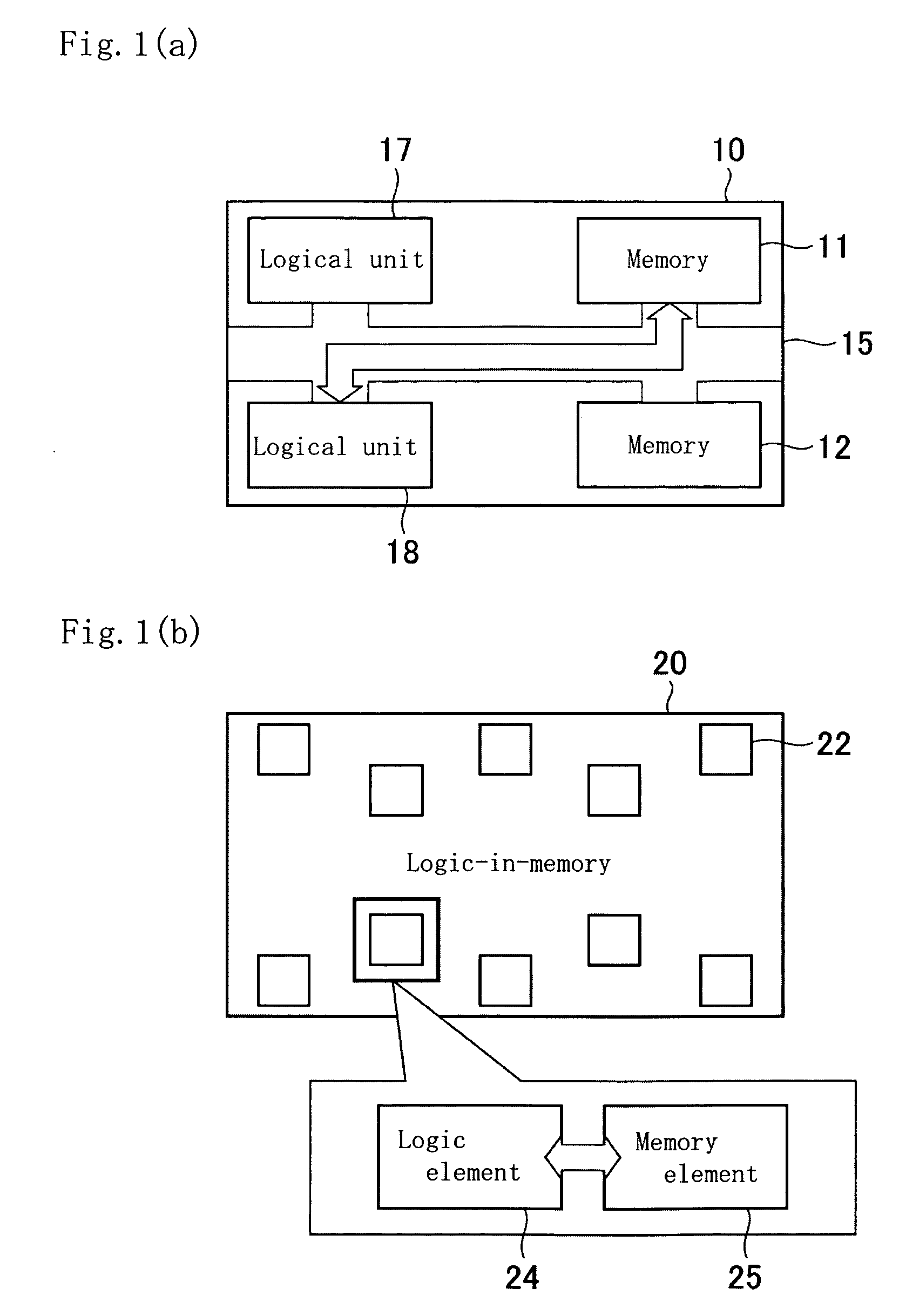
[0051] The logic-in-memory circuit 100 shown in FIG. 4 has binary inputs, i.e., an external input X and a memory input Y, and comprises an operation function for performing an operation f(X, Y) using the inputs X and Y and a memory function for storing the memory input Y. The operation result is obtained as a binary output Z. This kind of logic-in-memory circuit 100 consists of a TMR network 120 that includes TMR elements having operation functions and memory functions, a threshold detector 160 and an IV converter 170.

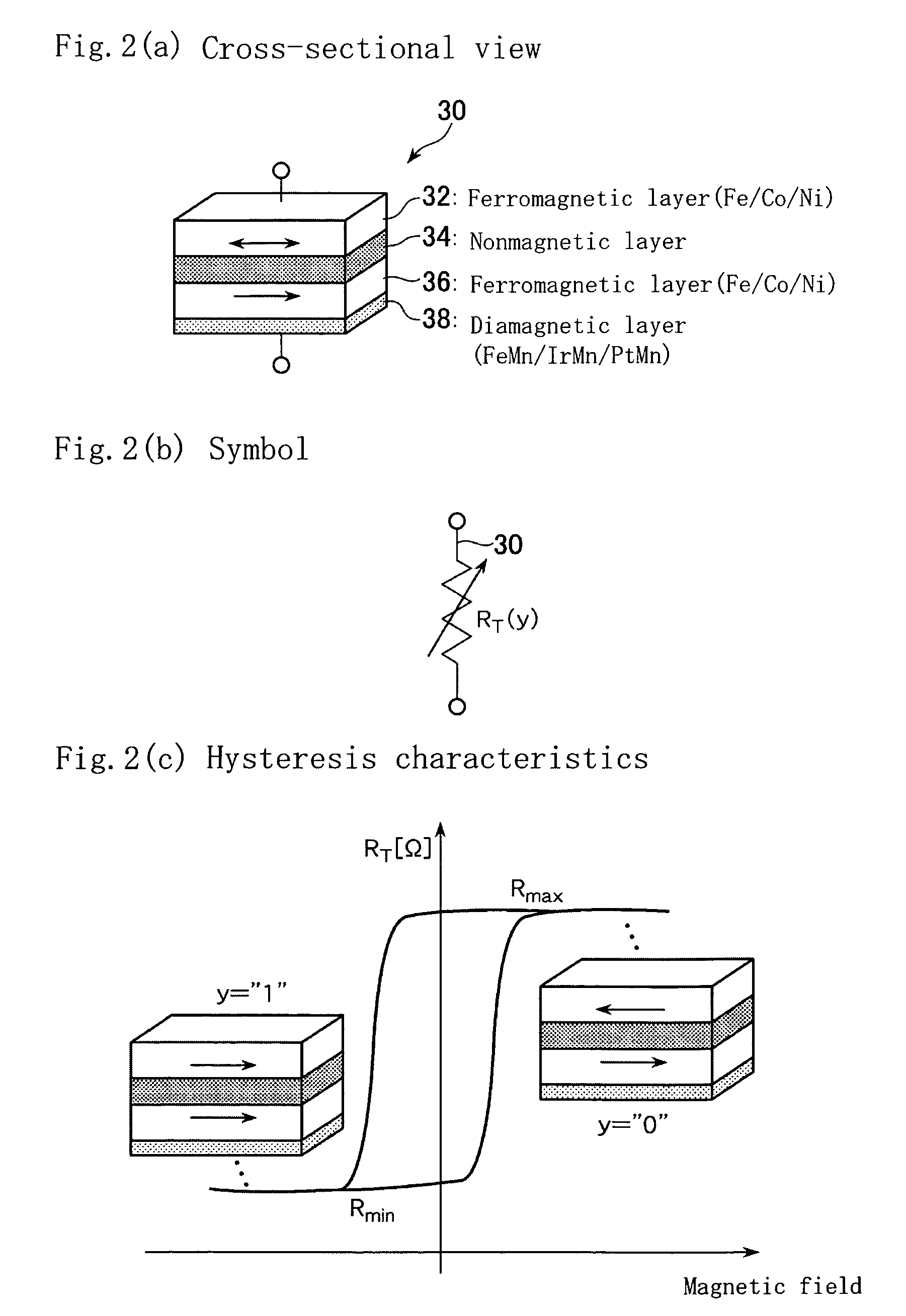
[0052] As shown, for example, in an AND operation network 122 in FIG. 5(b), the TMR network 120 is formed as a variable resistive element network by a series-parallel connection ...


PUM


Abstract

A TMR network 120 using TMR elements as magnetoresistive elements is formed as a variable resistive element network by a series-parallel connection of two kinds of variable resistive elements R with resistance values that change according to an external input X or a memory input Y, as shown in an AND operation network 122 in FIG. 5(b), wherein the total resistance value Rtotal is minimized, that is, the current I is maximized for a particular combination of the inputs. Assuming Rxi and Ryi (i=0, 1 and 2) as the resistance values of the variable resistive elements R according, respectively, to the external input X and memory input Y, the values of x and y determine the current I that flows through the network as shown in FIG. 5(d). Setting a threshold value between I0 and I1 using a threshold detector 160 makes it possible to realize AND operation. The operation result is then output as a voltage value through an IV converter 170.

Description

BACKGROUND OF THE INVENTION [0001] 1. Field of the Invention [0002] The present invention relates to a logic-in-memory circuit using magnetoresistive element, i.e., variable resistive element capable of storing information. [0003] 2. Description of the Related Art [0004] In integrated circuits where the performance improvement of processor elements, memories, etc. is promoted with the backdrop of rapid development in fine processing technology in recent years, performance degradation due to wiring delay and increasing wiring area is becoming a serious problem. From the point of view that many of these wiring related problems arise from conventional architectures in which circuits are formed with operation functions and memory functions being separated from each other, the inventors have focused on the logic-in-memory architecture, in which systems are formed with the integration of processor elements and memories, as a method for solving the wiring related problems fundamentally, an...

Claims


Application Information

Patent Timeline
IPC IPC(8): G11C11/00G11C11/15H01L21/8246H01L27/10H01L27/105H01L43/08H03K19/18
CPCG11C11/5607G11C11/15
Inventor HANYU, TAKAHIROKIMURA, HIROMITSU
Owner TOHOKU UNIV
Why Eureka
Try Eureka