

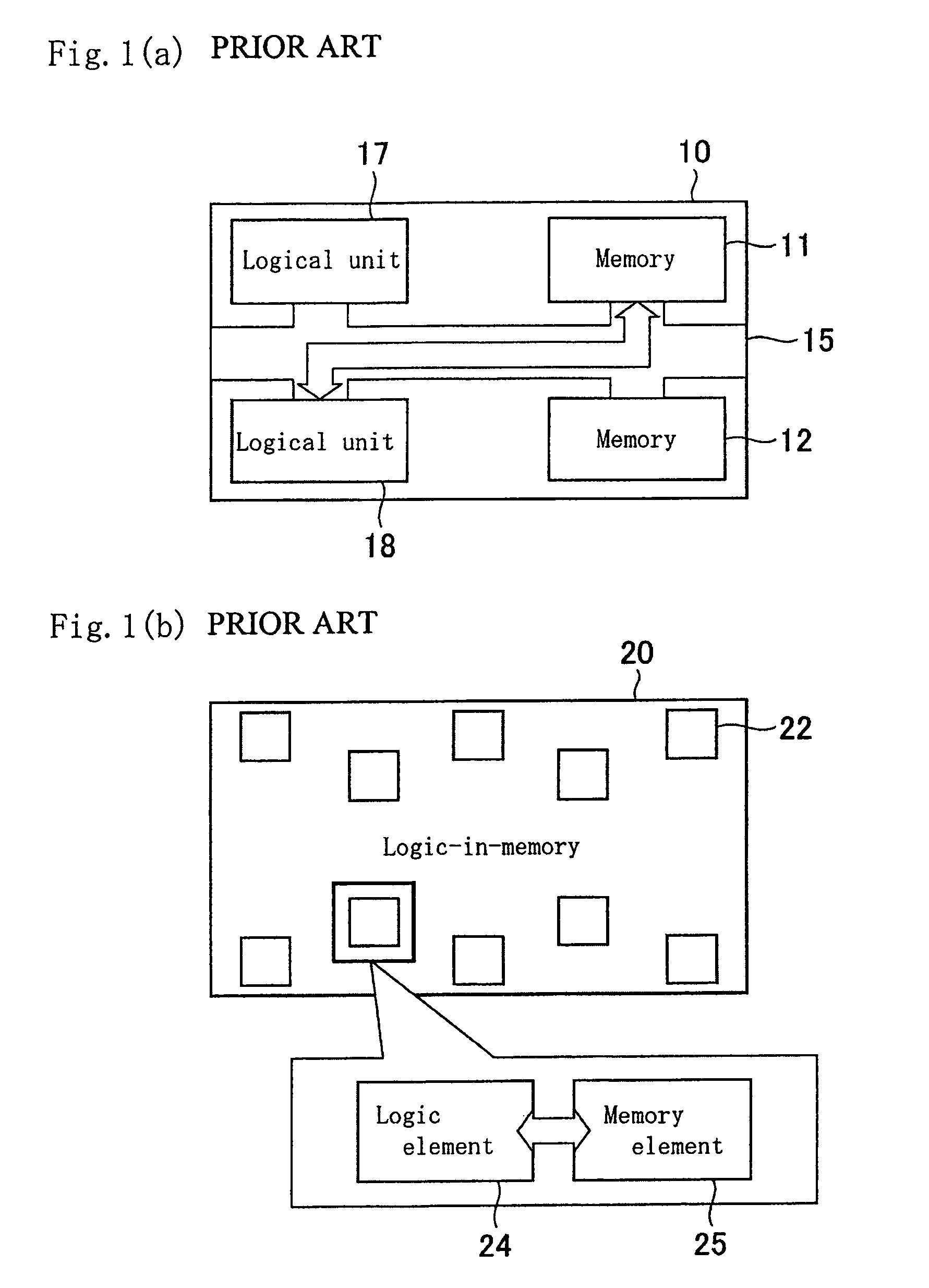
Logic-in-memory circuit using magnetoresistive element
a technology of magnetoresistive elements and logic-in-memory circuits, which is applied in the direction of solid-state devices, pulse techniques, instruments, etc., can solve the problems of performance degradation due to wiring delay and increasing wiring area, and achieve the effect of compact integration of excellent memory functions of magnetoresistive elements and minimal resistance value of network
- Summary
- Abstract
- Description
- Claims
- Application Information
AI Technical Summary
Benefits of technology
Problems solved by technology
Method used
Image

Examples
Embodiment Construction
[0049]Preferred embodiments of the present invention will hereinafter be described referring to the accompanying drawings.
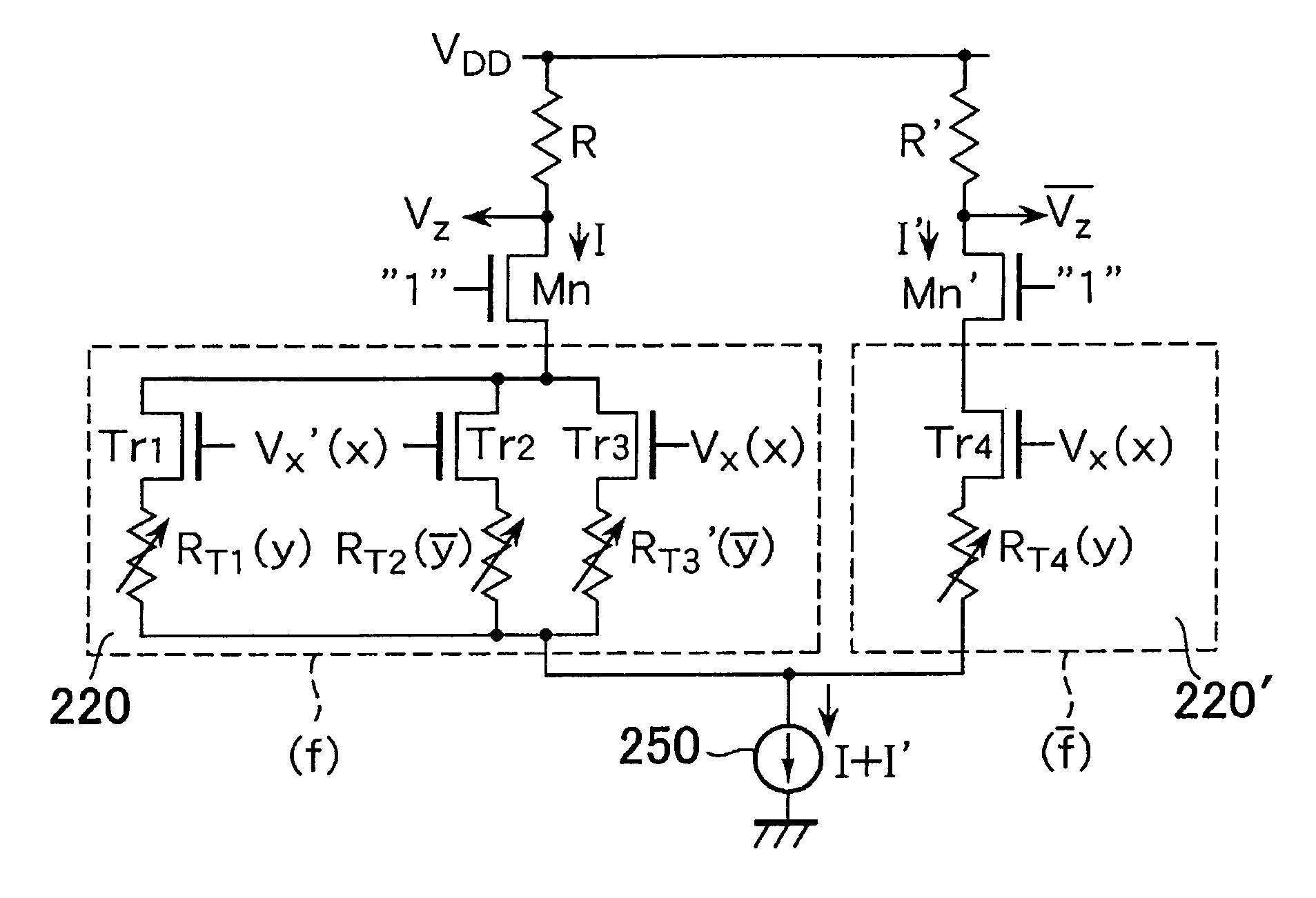
[0050]FIG. 4 is a view showing the overall configuration of a logic-in-memory circuit using TMR elements as magnetoresistive elements, i.e., variable resistive elements.
[0051]The logic-in-memory circuit 100 shown in FIG. 4 has binary inputs, i.e., an external input X and a memory input Y, and comprises an operation function for performing an operation f (X, Y) using the inputs X and Y and a memory function for storing the memory input Y. The operation result is obtained as a binary output Z. This kind of logic-in-memory circuit 100 consists of a TMR network 120 that includes TMR elements having operation functions and memory functions, a threshold detector 160 and an IV converter 170.
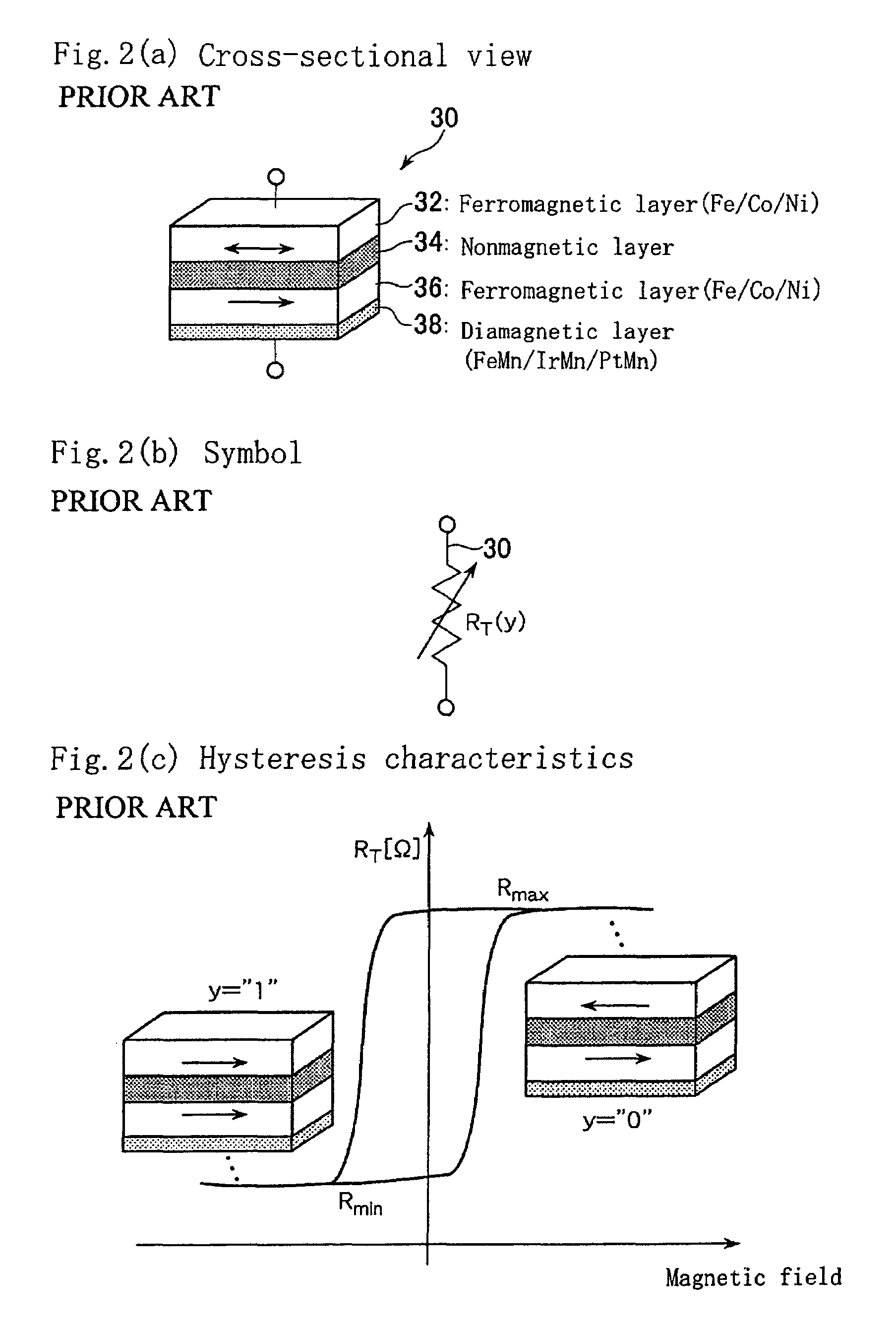
[0052]As shown, for example, in an AND operation network 122 in FIG. 5(b), the TMR network 120 is formed as a variable resistive element network by a series-parallel connection of tw...
PUM
 Abstract
Description
Claims
Application Information