

Three dimensional integrated circuits
a three-dimensional integrated circuit and integrated circuit technology, applied in the direction of electrical equipment, semiconductor devices, semiconductor/solid-state device details, etc., can solve the problems of low areal and vertical density, high electrical impedance between individual chips, and multiple significant limitations of the multi-chip 2-dimensional module approach currently used in the integrated circuit industry for interconnecting chips into electronic systems
- Summary
- Abstract
- Description
- Claims
- Application Information
AI Technical Summary
Benefits of technology
Problems solved by technology
Method used
Image

Examples
Embodiment Construction
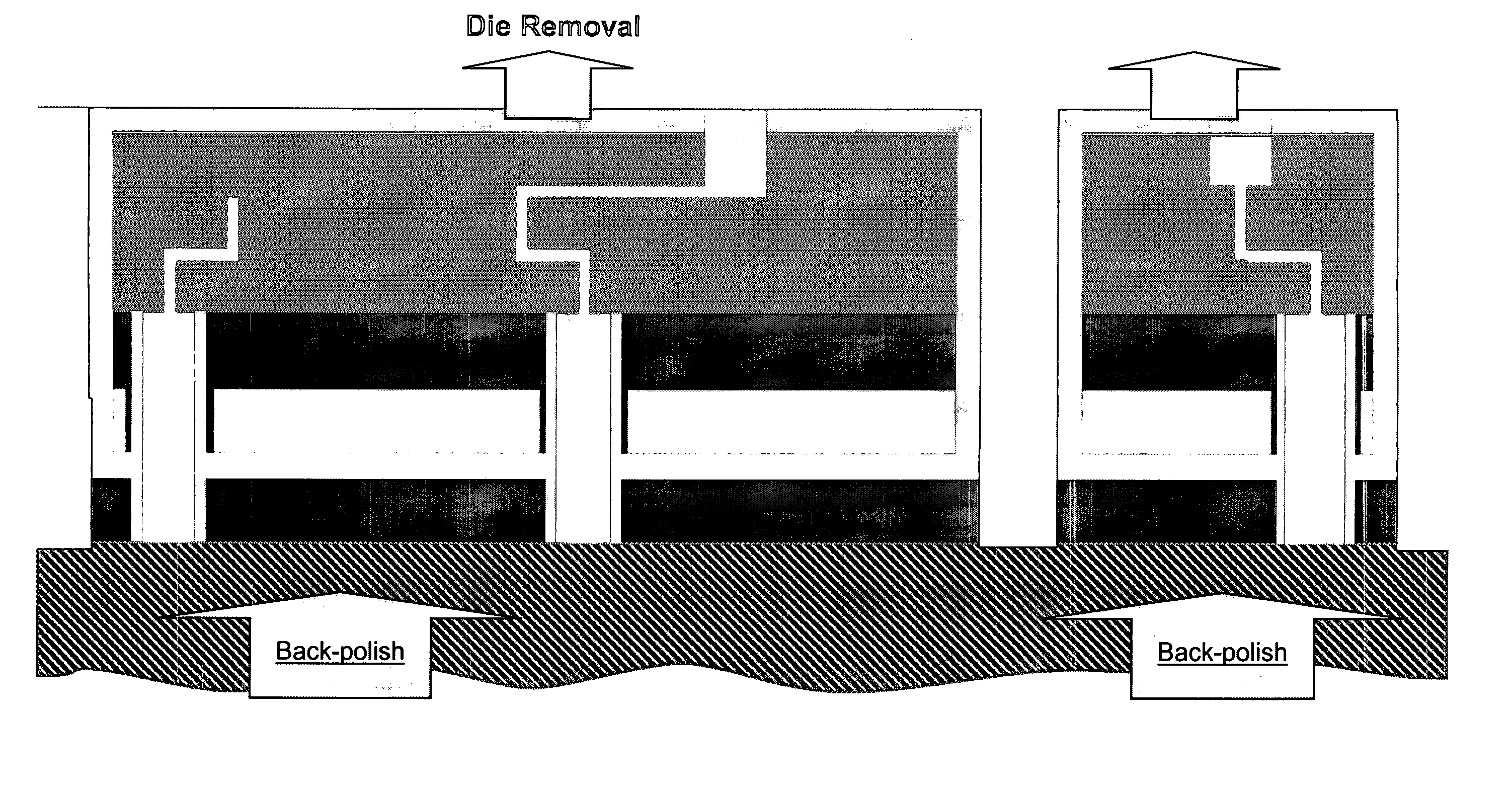
[0016] The invention relates to a three dimensional (3d) integrated circuit and to a method for fabricating a three dimensional integrated circuit system. The 3d circuit comprises two or more integrated circuits, each integrated circuit being at least partially separated from an adjacent integrated circuit by a cooling channel. At least two integrated circuits are electrically connected.
[0017] The 3d circuit is fabricated by: forming an integrated circuit; and stacking two or more integrated circuits such that at least two of the stacked circuits are electrically connected.
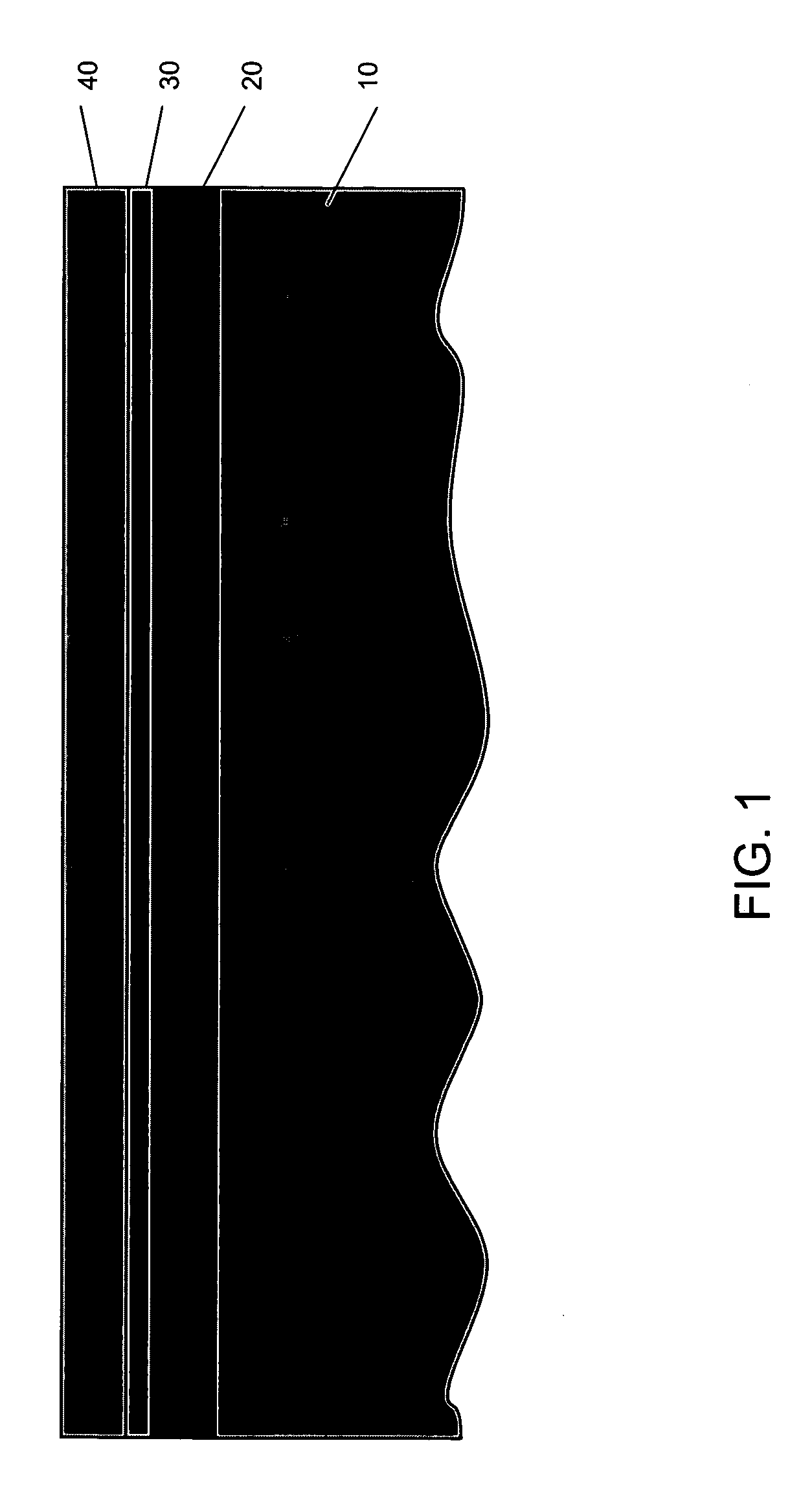
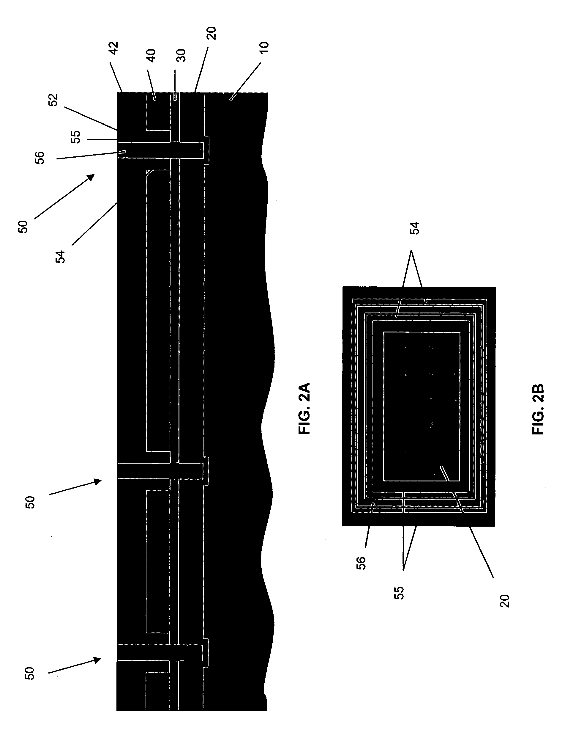
[0018] The step of creating an integrated circuit comprises: providing a substrate, a sacrificial layer overlying a surface of the substrate (or the sacrificial layer may be a sacrificial portion of the substrate), a first protective layer overlying the sacrificial layer, and a semiconductor layer overlying the first protective layer; forming circuitry in the semiconductor layer to provide an active layer; formi...
PUM
 Abstract
Description
Claims
Application Information