Field-effect transistor

Inactive Publication Date: 2006-03-02
NEC CORP
View PDF4 Cites 81 Cited by
  • Summary
  • Abstract
  • Description
  • Claims
  • Application Information

AI Technical Summary

Benefits of technology

[0048] As described above, in the field-effect transistor of the present invention, the suppression of the collapse and the higher gate breakdown volt

Problems solved by technology

Namely, there is a trade-off between the amount of collapse and the gate breakdown voltage, and the control becomes extremely difficult. FIG. 19 shows an evaluation result of a relationship among a thickness of the surface protection film SiN, the amount of collapse, and the gate breakdown voltage, which was obtained by using a prototype of HJFET having the structure of FIG. 17 in which the electric-field control electrode is not provided.
However, when the SiN film is thickened, the surfa

Method used


Image

  • Field-effect transistor
  • Field-effect transistor
  • Field-effect transistor

Examples


Example

EXAMPLE 1

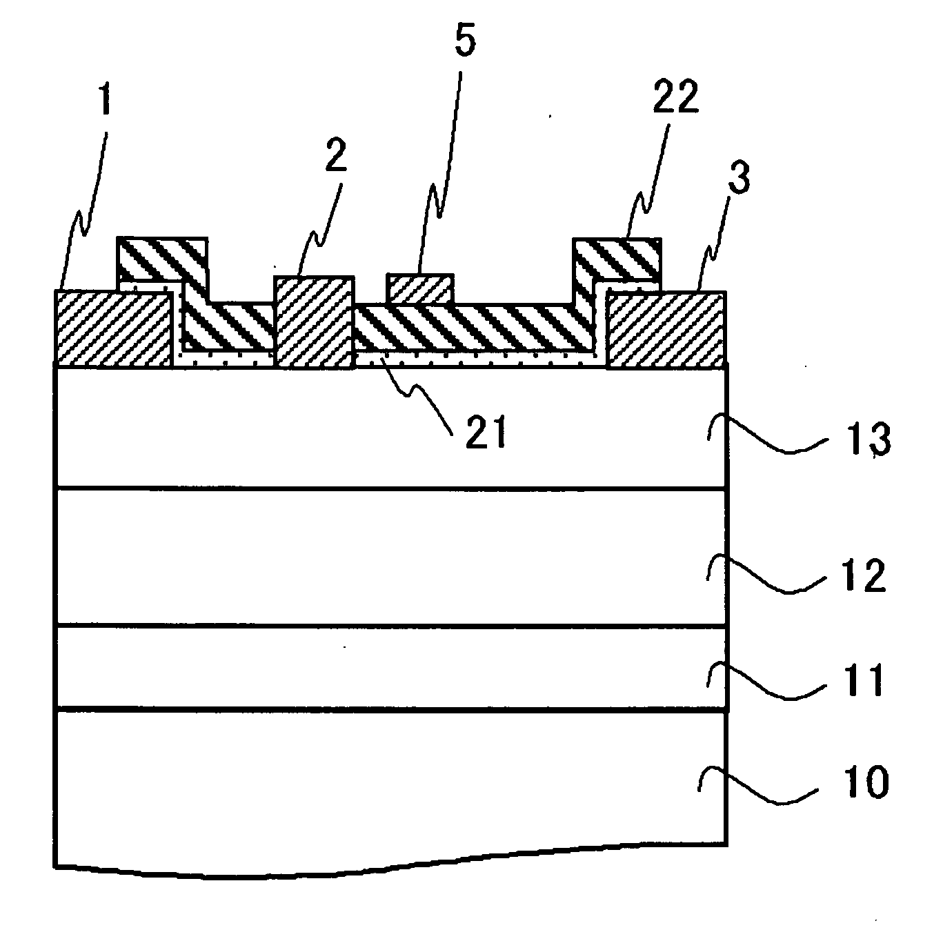
[0082]FIG. 1 shows a sectional structure of HJFET in Example 1. HJFET is formed on a substrate 10 made of a material such as SiC. A buffer layer 11 including a semiconductor layer is formed on the substrate 10. A GaN channel layer 12 is formed on the buffer layer 11. An AlGaN electron supply layer 13 is formed on the channel layer. A source electrode 1 and a drain electrode 3, in which ohmic contact is secured, are formed on the electron supply layer. A gate electrode 2, in which Schottky contact is secured, and an electric-field control electrode 5 are provided between the source electrode 1 and the drain electrode 3. A surface of the electron supply layer 13 is covered with a SiN film 21, and a SiO2 film 22 is further provided on the SiN film 21. The SiN film 21 and the SiO2 film 22 are provided immediately below the electric-field control electrode 5.

[0083] Referring to FIGS. 21 to 23, a method of manufacturing HJFET according to Example 1 will be described below. At f...

Example

EXAMPLE 2

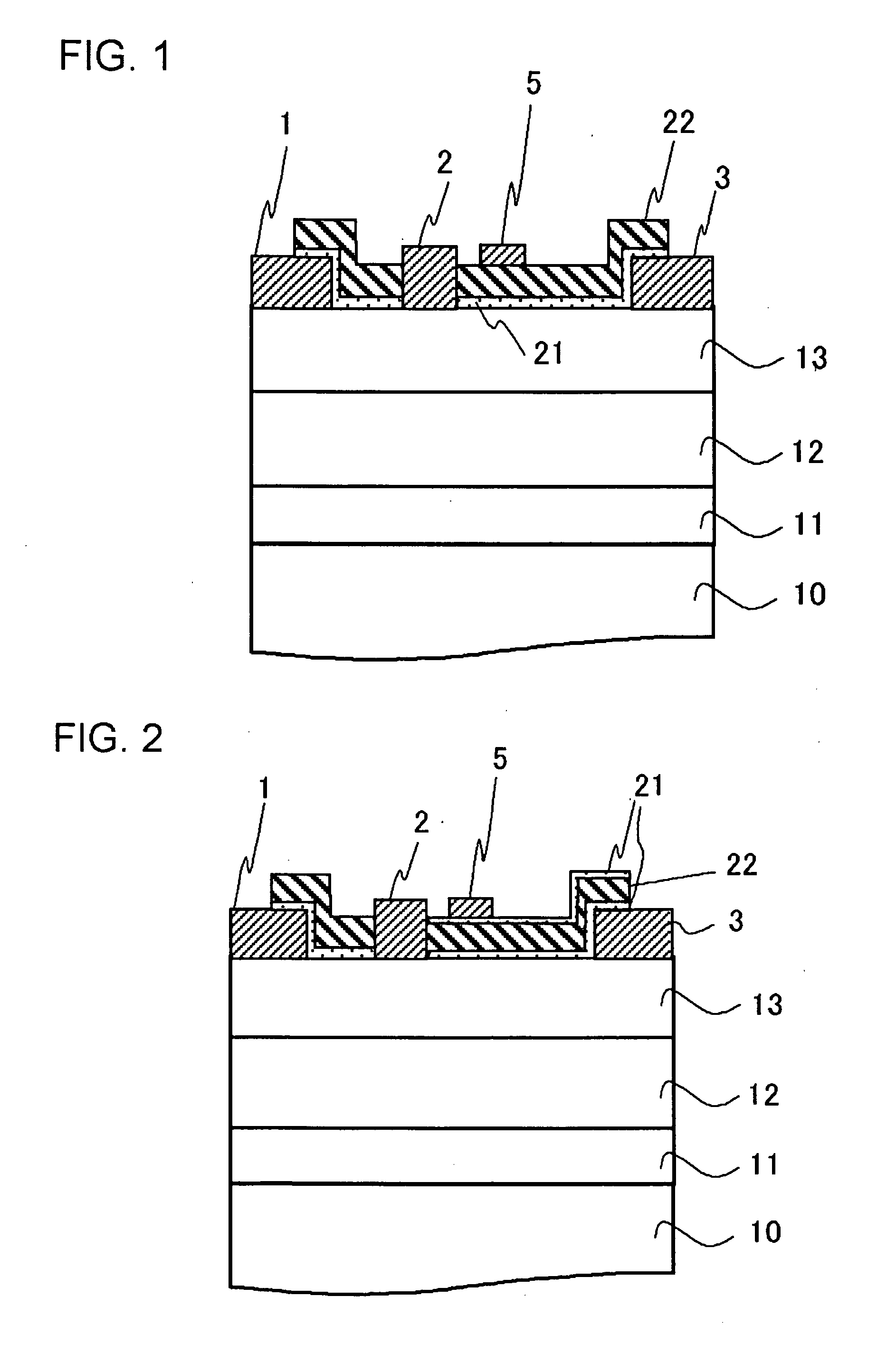
[0091] In Example 2, as shown in FIG. 2, the insulating film is formed on the AlGaN electron supply layer 13 (on the Group III nitride semiconductor layer), and has a three-layer structure in which the SiN film 21, the SiO2 film 22, and the SiN film 21 are sequentially laminated. The semiconductor layer structure below the gate electrode is similar to Example 1. In the structure of Example 2, the uppermost layer of the insulating film is formed not by the SiO2 film 22 but by the SiN film 21, so that the resist is easily stably formed to improve the yield in the process of manufacturing the element. In this case, as with the SiN film provided in the lowermost layer, from the viewpoint of the film reliability, it is preferable that the insulating film provided in the uppermost portion of the insulating film is set at the film thicknesses not more than 150 nm, and it is more preferable that the insulating film is set at the film thicknesses not more than 100 nm. Further, it i...

Example

EXAMPLE 3

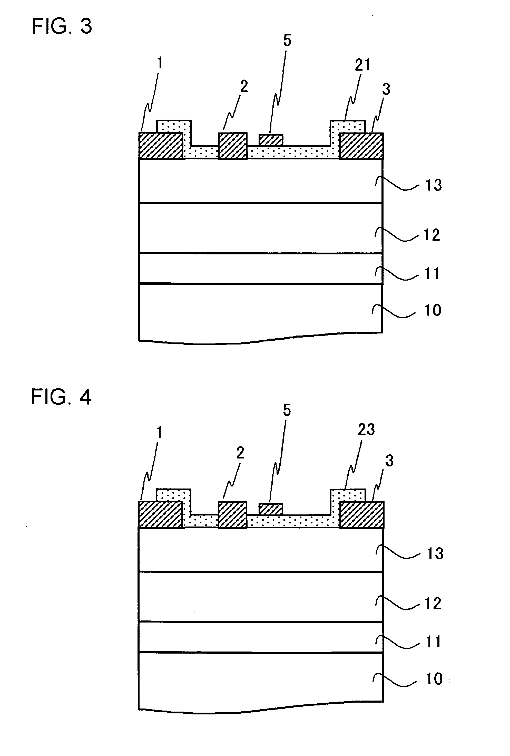
[0092]FIG. 3 shows a sectional structure of HJFET in Example 3. HJFET is formed on the substrate 10 made of the material such as SiC. The buffer layer 11 including the semiconductor layer is formed on the substrate 10. The GaN channel layer 12 is formed on the buffer layer 11. The AlGaN electron supply layer 13 is formed on the channel layer. The source electrode 1 and the drain electrode 3, in which the ohmic contact is secured, are formed on the electron supply layer. The gate electrode 2, in which the Schottky contact is secured, and the electric-field control electrode 5 are provided between the source electrode 1 and the drain electrode 3. The surface of the electron supply layer 13 is covered with the SiN film 21, and the SiN film 21 is provided immediately below the electric-field control electrode 5.

[0093] HJFET according to Example 2 is formed as follows: At first, the semiconductor is grown on the substrate 10 made of SiC by the molecular beam epitaxy growth met...


PUM


Abstract

An electric-field control electrode (5) is formed between a gate electrode (2) and a drain electrode (3). A multilayered film including a SiN film (21) and a SiO2 film (22) is formed below the electric-field control electrode (5). The SiN film (21) is formed so that a surface of an AlGaN electron supply layer (13) is covered with the SiN film (21).

Description

FIELD OF THE INVENTION [0001] The present invention relates to a field-effect transistor in which a Group III nitride semiconductor is used. DESCRIPTION OF THE RELATED ART [0002] Group III nitride semiconductors including GaN have a large band gap, a high dielectric breakdown electric field, and high electron saturation drift velocity. Further, because two-dimensional carrier gas can be utilized by a heterojunction, the Group III nitride semiconductors are expected as a material for realizing an electronic element which is excellent for high-temperature operation, high-speed switching operation, large-power operation, and the like. [0003] In the transistor in which the Group III nitride semiconductor is used, the large amount of negative charge is generated in the substrate surface, which largely affects transistor performance. This respect will be described below. [0004] When AlGaN is grown on undoped GaN, a positive fixed charge is generated in a hetero-interface by actions of bot...

Claims


Application Information

Patent Timeline
IPC IPC(8): H01L31/0328H01L21/336H01L29/812H01L21/338H01L29/06H01L29/20H01L29/40H01L29/778H01L29/80
CPCH01L29/2003H01L29/7787H01L29/402
Inventor OKAMOTO, YASUHIROMIYAMOTO, HIRONOBUANDO, YUJINAKAYAMA, TATSUOINOUE, TAKASHIKUZUHARA, MASAAKI
Owner NEC CORP
Why Eureka
Try Eureka