
Enhanced GaN-based high electron mobility transistor and preparation method thereof

A high electron mobility, transistor technology, applied in semiconductor/solid state device manufacturing, circuits, electrical components, etc., can solve the problems affecting the performance of HEMT devices, existing off-state leakage current, reducing device performance, etc., to reduce the off-state Effect of leakage current, reduction of off-state leakage current, effect of large forward gate voltage

Pending Publication Date: 2021-06-11
NANTONG UNIVERSITY
View PDF0 Cites 1 Cited by
  • Summary
  • Abstract
  • Description
  • Claims
  • Application Information

AI Technical Summary

Problems solved by technology

However, GaN materials inevitably have defects during the growth process, and these defects will affect the performance of HEMT devices
The threshold voltage of traditional p-GaN gate structure HETM devices is low, and there is room for improvement in gate breakdown voltage, and due to the existence of defects, there will be off-state leakage current, thereby reducing device performance

Method used


Image

  • Enhanced GaN-based high electron mobility transistor and preparation method thereof
  • Enhanced GaN-based high electron mobility transistor and preparation method thereof
  • Enhanced GaN-based high electron mobility transistor and preparation method thereof

Examples


Embodiment 1

[0045] Example 1 Preparation Method of Enhanced GaN-Based High Electron Mobility Transistor

[0046] The first step is to clean the material.

[0047]First, put the sample into the mixture of concentrated sulfuric acid and hydrogen peroxide (concentrated sulfuric acid:hydrogen peroxide=7:3) and soak for 10 minutes. Then put the sample into the diluted ammonia (20%) and hydrogen peroxide mixture (diluted ammonia:hydrogen peroxide=6:1), heat in a water bath for 10 minutes, and set the temperature of the water bath to 85°C. Then put the sample into the aqueous solution of KOH: hydrogen peroxide = 1:2 and soak for 10 minutes, and finally wash it with deionized water. Cleaning the sample with the above-mentioned series of acid and alkali solutions can effectively remove oxides on the surface of the sample, as well as compounds and impurities that are poorly soluble in acetone. Afterwards, the sample is subjected to a traditional cleaning step. First, the sample is placed in aceto...

Embodiment 2

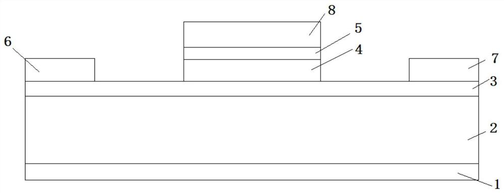
[0068] like figure 1 and Figure 5 As shown, the enhancement mode GaN-based high electron mobility transistor, its structure includes from bottom to top:

[0069] A sapphire substrate layer 1;

[0070] A GaN buffer layer 2, unintentionally doped, with a thickness of 2 μm;

[0071] An AlGaN barrier layer 3 with an Al composition of 0.25 and a thickness of 20 nm;

[0072] An annular p-GaN layer 4 with a Mg doping concentration of 5*10 19 cm -3 , with a thickness of 50nm;

[0073] a ring Ga 2 o 3 Layer 5, the length and width are consistent with the p-GaN layer, and the thickness is 5nm;

[0074] The source electrode 6 and the drain electrode 7 are arranged on the AlGaN barrier layer and are ohmic contacts;

[0075] Ring-shaped gate electrode 8, set on Ga 2 o 3 layer, is a Schottky contact, and the length and width are related to Ga 2 o 3 The layers are consistent and are disposed between the source and drain electrodes, spacing them apart.

[0076] Detect the condu...

Embodiment 3

[0085] like Image 6 As shown, the enhancement mode GaN-based high electron mobility transistor, its structure includes from bottom to top:

[0086] - Si substrate layer;

[0087] A GaN buffer layer, unintentionally doped, with a thickness of 1 μm;

[0088] An AlGaN barrier layer with an Al composition of 0.2 and a thickness of 15 nm;

[0089] Strip p-GaN layer with Mg doping concentration of 1*10 19 cm -3 , with a thickness of 40nm;

[0090] Strip Ga 2 o 3 layer, the length and width are consistent with the p-GaN layer, and the thickness is 3nm;

[0091] The source electrode and the drain electrode are arranged on the AlGaN barrier layer and are ohmic contacts;

[0092] Strip gate electrodes, set on Ga 2 o 3 layer, is a Schottky contact, and the length and width are related to Ga 2 o3 The layers are consistent and are disposed between the source and drain electrodes, spacing them apart.


PUM

PropertyMeasurementUnit
Thicknessaaaaaaaaaa
Thicknessaaaaaaaaaa
Layer thicknessaaaaaaaaaa

Abstract

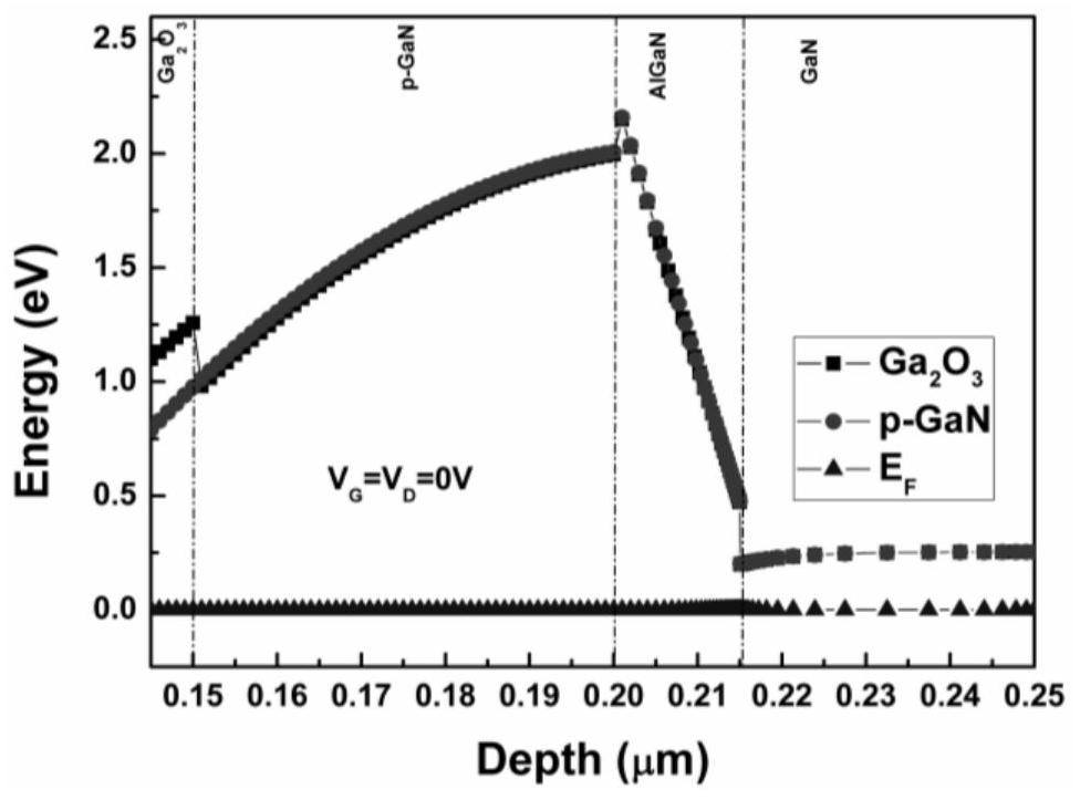
The invention discloses an enhanced GaN-based high-electron-mobility transistor, which sequentially comprises a substrate layer, a GaN buffer layer, an AlGaN potential barrier layer, a p-GaN layer, a Ga2O3 layer, a source electrode, a drain electrode and a gate electrode from bottom to top, wherein the length and the width of the Ga2O3 layer are consistent with those of the p-GaN layer, the source electrode and the drain electrode are disposed on the AlGaN barrier layer, and the gate electrode is arranged on the Ga2O3 layer, is consistent with the Ga2O3 layer in length and width, and is used for separating the source electrode from the drain electrode. The invention further discloses a preparation method. In the HEMT device structure, due to the spontaneous polarization and piezoelectric polarization effects of the GaN material, 2DEG can be formed between the GaN layer and the AlGaN layer; when the bias voltage is zero, the p-GaN layer can exhaust the 2DEG in the channel, so that the device obtains enhanced performance; gallium oxide and p-GaN form a p-n junction under the gate, and the p-n junction and the gate jointly regulate and control channel carriers; the forward threshold voltage of the device is improved; the gate breakdown voltage of the device is improved; and the off-state leakage current of the device is reduced.

Description

technical field [0001] The invention relates to an enhanced GaN-based high electron mobility transistor and a preparation method thereof, belonging to the technical field of semiconductor devices. Background technique [0002] Group III nitride semiconductor materials are the third-generation semiconductor materials. They have large band gap, high electron saturation velocity, high temperature resistance, high voltage resistance, and radiation resistance. They are ideal materials for the preparation of power electronic devices. GaN-based high-mobility transistors (HEMTs) have broader application prospects in high-temperature, high-frequency, and high-power fields than power electronic devices based on Si and GaAs materials. AlGaN / GaN heterojunction is the basic structure of GaN-based HEMT devices. Due to the unique spontaneous polarization and piezoelectric polarization effects of GaN materials, a high concentration of two-dimensional electron gas (2DEG) naturally exists in ...

Claims


Application Information

Patent Timeline
IPC IPC(8): H01L29/778H01L21/335H01L29/20H01L29/06
CPCH01L29/778H01L29/66462H01L29/2003H01L29/0611
Inventor 葛梅
Owner NANTONG UNIVERSITY
Learn More