Trench gate type transistor
a transistor and gate gate technology, applied in the direction of basic electric elements, electrical equipment, semiconductor devices, etc., to achieve the effects of reducing gate capacitance, preventing crystal defects, and enhancing gate breakdown voltag
- Summary
- Abstract
- Description
- Claims
- Application Information
AI Technical Summary
Benefits of technology
Problems solved by technology
Method used
Image
Examples
first embodiment
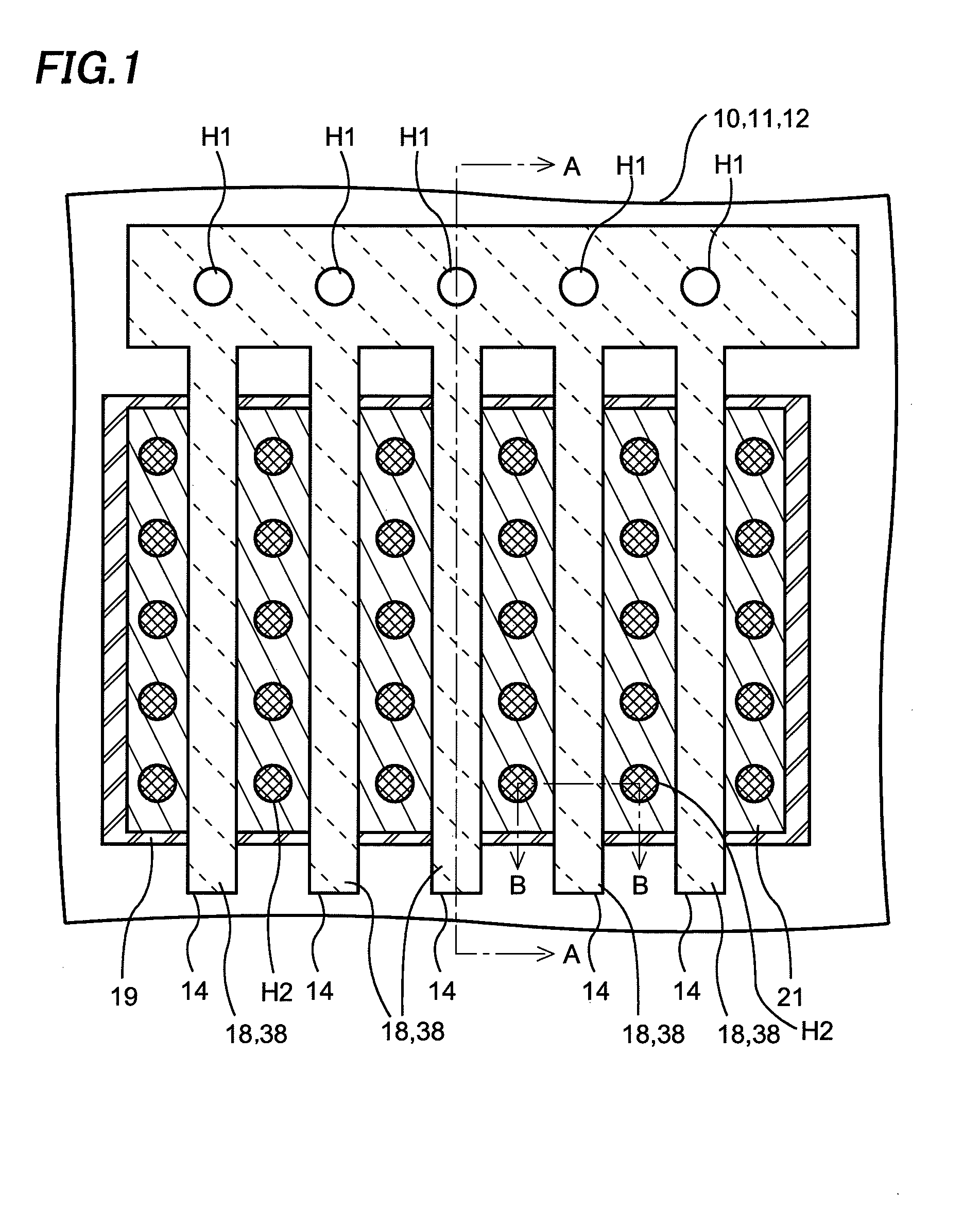
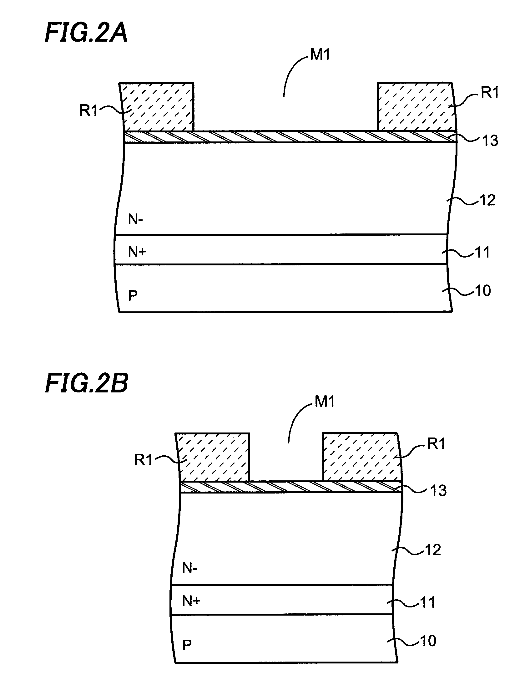
[0019]A first embodiment of the invention will be described referring to figures. FIG. 1 is a plan view for explaining a trench gate type transistor and a method of manufacturing the same of the embodiment of the invention. FIGS. 2(A) to 14(A) are cross-sectional views of FIG. 1 along line A-A, and FIGS. 2(B) to 14(B) are cross-sectional views of FIG. 1 along line B-B. In the following description, the trench gate type transistor is referred to as a transistor simply. The conductive type of this transistor is not limited, but the following description is given for a case of an N channel type transistor.
[0020]First, the schematic plan structure of the transistor of the embodiment will be described referring to FIG. 1. Here, only main elements will be described. In this transistor, an N+ type semiconductor layer 11 and an N− type semiconductor layer 12 are formed on a P type semiconductor substrate 10, and a plurality of trenches 14 each having short sides and long sides is formed in ...
second embodiment
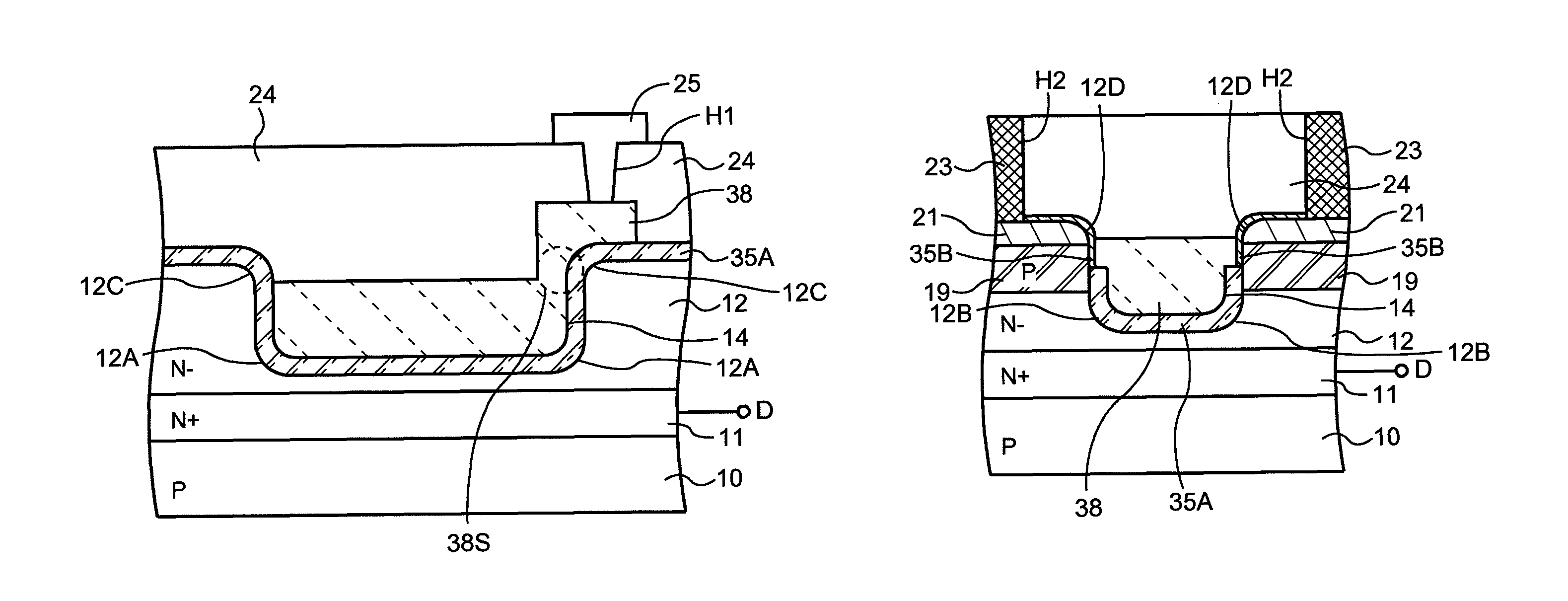
[0043]A second embodiment of the invention will be described referring to figures. The schematic plan structure of this transistor is the same as that of FIG. 1.
[0044]Hereafter, a trench gate type transistor and a method of manufacturing the same of the embodiment will be described referring to figures. FIGS. 17(A) to 26(A) are cross-sectional views of FIG. 1 along line A-A, and FIGS. 17(B) to 26(B) are cross-sectional views of FIG. 1 along line B-B. In FIGS. 17 to 26, the same numerals are given to the same elements as those of FIGS. 2 to 14.
[0045]First, in the similar manner to the processes shown in FIGS. 2 to 5 in the first embodiment, an N+ type semiconductor layer 11 and an N− type semiconductor layer 12 are formed on a semiconductor substrate 10, and trenches 14 are formed in the N− type semiconductor layer 12. A silicon oxide film 35A which corresponds to the silicon oxide film 15A, and a photoresist reinforcement film 36 which corresponds to the photoresist reinforcement fi...
PUM
 Abstract
Description
Claims
Application Information


