Semiconductor device and method for manufacturing the same

Active Publication Date: 2012-05-10
MITSUBISHI ELECTRIC CORP
View PDF13 Cites 10 Cited by
  • Summary
  • Abstract
  • Description
  • Claims
  • Application Information

AI Technical Summary

Benefits of technology

[0008]An object of the present invention is to provide a semiconductor device capable of re

Problems solved by technology

The semiconductor devices disclosed in Japanese Patent No. 4049095 and Japanese Patent Application Laid-Open No. 2009-32919 involve a problem that the intensity of the electric field ap

Method used


Image

  • Semiconductor device and method for manufacturing the same
  • Semiconductor device and method for manufacturing the same
  • Semiconductor device and method for manufacturing the same

Examples


embodiment 1

A. Preferred Embodiment 1

[0038]Firstly, a background technique of a semiconductor device according to the present invention will be described.

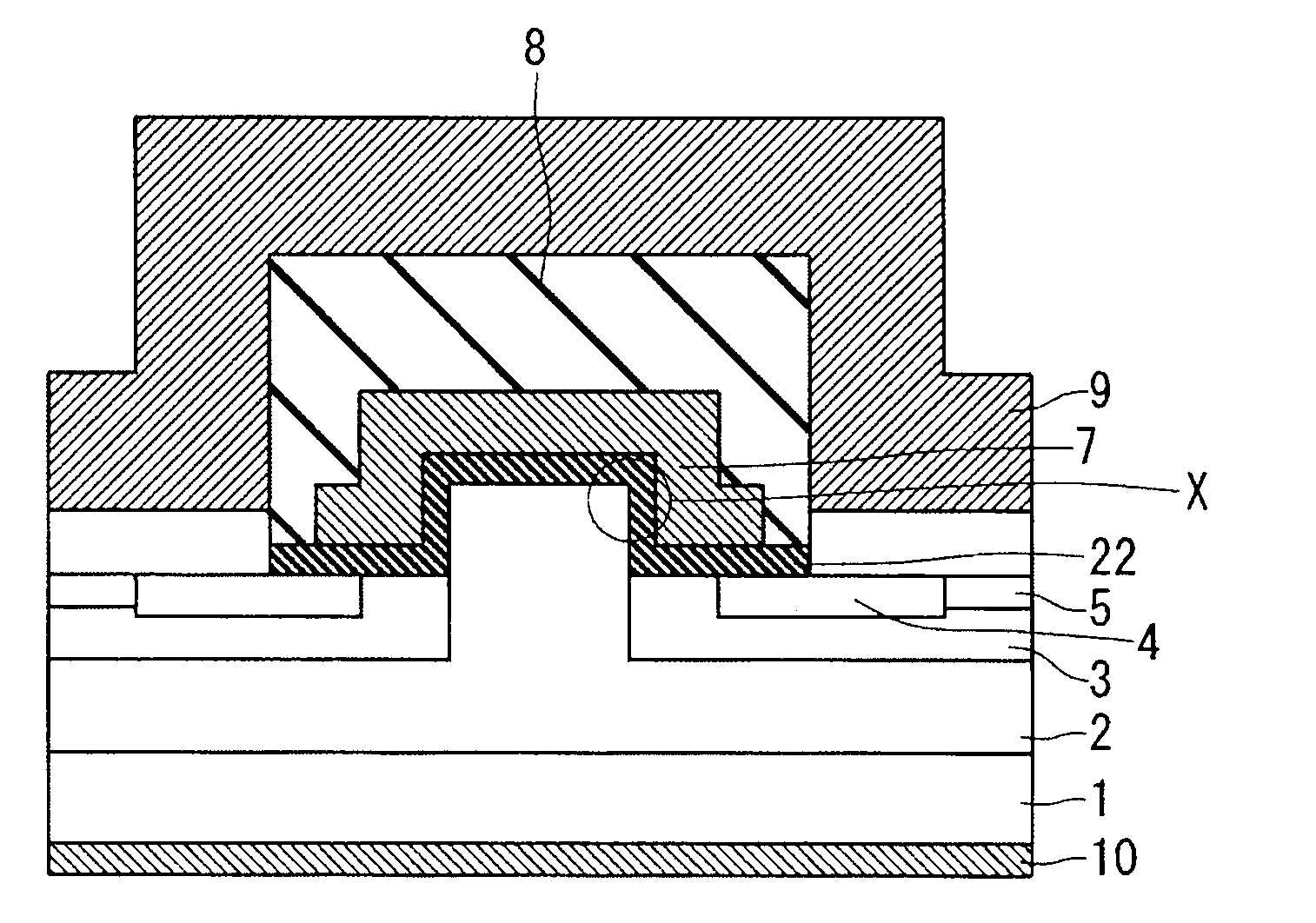
[0039]As shown in FIG. 25, in the semiconductor device according to the background technique of the present invention, an epitaxial layer 2 of a first conductive type (such as the N-type), which is a drift layer, is formed on a semiconductor substrate 1 of the first conductive type, and the epitaxial layer 2 has a protrusion interposed between grooves.

[0040]Well regions 3 of a second conductive type are formed on surfaces of the grooves of the epitaxial layer 2 such that the protrusion of the epitaxial layer 2 can be interposed between the well regions. Furthermore, a source region 4 of the first conductive type is selectively formed in a surface of the well region 3. A contact region 5 is formed on a surface of the epitaxial layer 2 so as to be adjacent to the source region 4.

[0041]As shown in FIG. 25, a gate insulating film 22 is formed so a...

embodiment 2

B. Preferred Embodiment 2

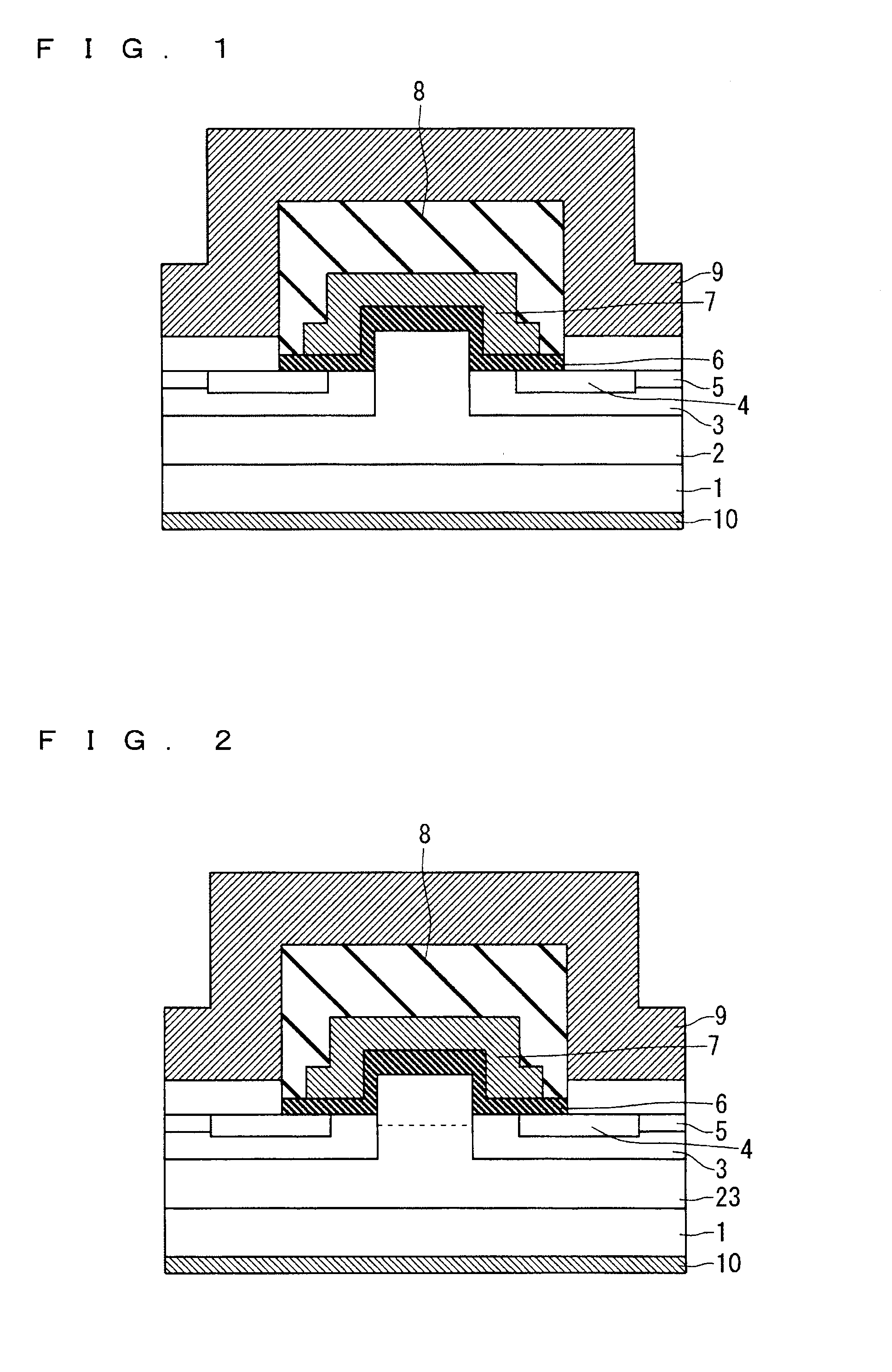
[0085]FIG. 18 shows a cross-section of a structure of a semiconductor device according to a preferred embodiment 2. This structure is identical to the structure shown in FIG. 1, except that a second conductive type region 27 or a semi-insulating region 28 is additionally formed between the upper surface of the protrusion and the gate insulating film 6.

[0086]This formation process makes it easy that the depletion layer in the JFET region extends, so that an electric field applied to the gate insulating film 6 in the JFET region can be further suppressed, and the gate capacitance can be reduced, too.

[0087]Although the epitaxial layer 2 is adopted in the example shown in FIG. 18, the epitaxial layer 23 may be used.

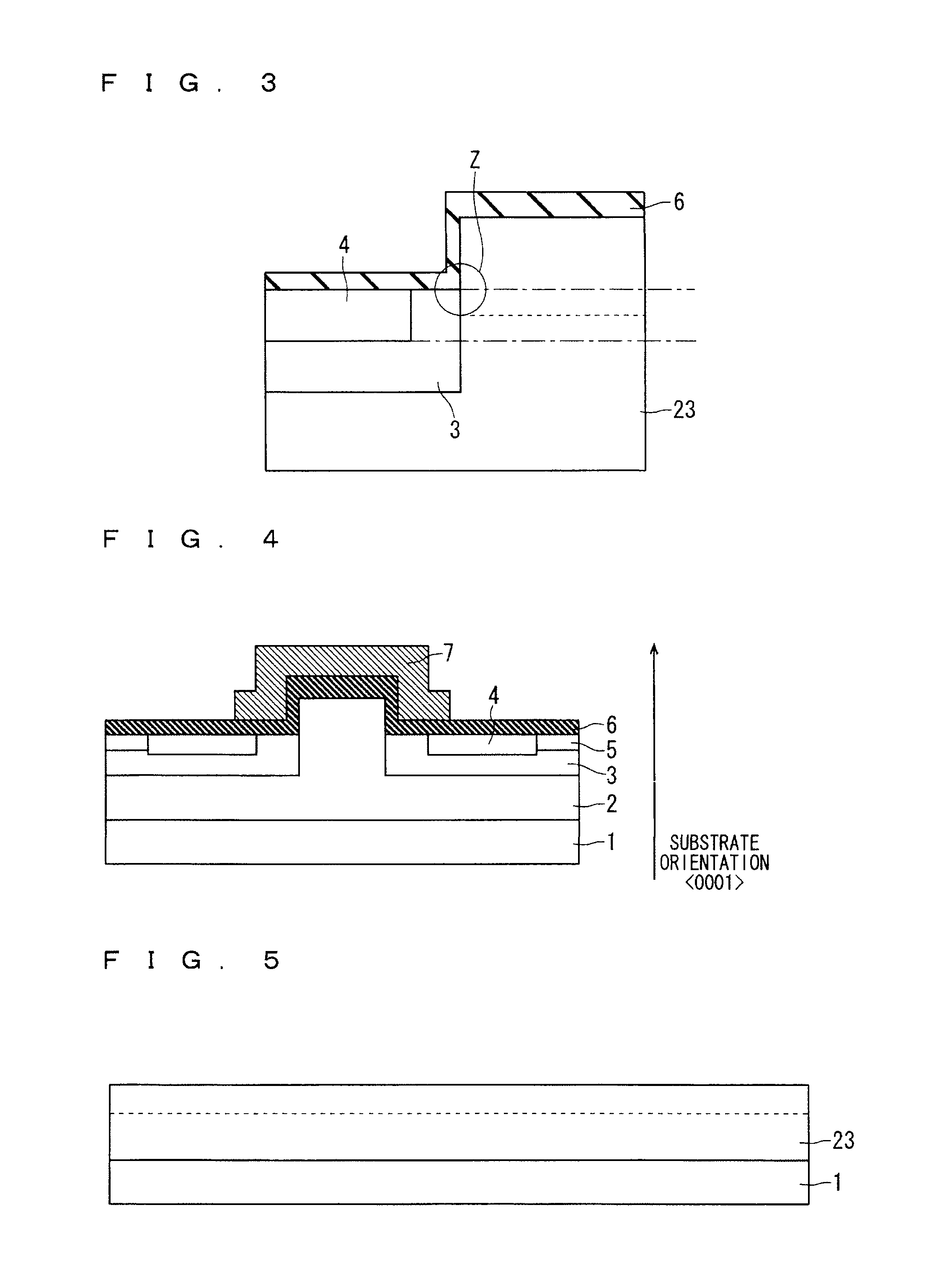
[0088]FIGS. 19 to 21 show a first method for manufacturing the semiconductor device according to the preferred embodiment 2. A basic flow thereof is identical to that of the preferred embodiment 1 shown in FIGS. 5 to 12, and therefore steps different ...


PUM


Abstract

A semiconductor device of the present invention includes: a semiconductor substrate of a first conductive type; an epitaxial layer of the first conductive type formed on the semiconductor substrate and having a protrusion formed on a surface thereof; a well region of a second conductive type formed on the surface of the epitaxial layer at each side of the protrusion; a source region of the first conductive type selectively formed in a surface of the well region; a gate insulating film formed so as to cover at least the protrusion and the surface of the well region; and a gate electrode formed on a part of the gate insulating film corresponding to the protrusion. The gate insulating film is thicker in a region thereof corresponding to an upper surface of the protrusion than the other regions thereof.

Description

BACKGROUND OF THE INVENTION[0001]1. Field of the Invention[0002]The present invention relates to a semiconductor device and a method for manufacturing the semiconductor device, and particularly to a reduction in a field and in a gate capacitance of a gate insulating film in a JFET region of a MOSFET.[0003]2. Description of the Background Art[0004]According to Japanese Patent No. 4049095 disclosing a semiconductor device, a groove (protrusion) is formed on a surface of a drift region, and a p-well region is formed in a bottom portion of the groove. A gate insulating film is thicker at a side surface of the groove than at other portions.[0005]In such a configuration, the gate insulating film in a JFET region is arranged on an upper side of the protrusion of the groove, to thereby suppress an electric field that is applied to the gate insulating film in the JFET region when a high voltage is applied to the drain side while a MOSFET is OFF.[0006]According to Japanese Patent Application ...

Claims


Application Information

Patent Timeline
IPC IPC(8): H01L29/78H01L21/336
CPCH01L23/544H01L29/0657H01L29/0878H01L29/1608H01L29/167H01L29/41766H01L29/42368H01L2924/0002H01L29/66068H01L29/7802H01L2223/54426H01L2223/54453H01L2924/00H01L29/66712
Inventor TARUI, YOICHIRO
Owner MITSUBISHI ELECTRIC CORP
Why Eureka
Try Eureka