Semiconductor device and method of manufacturing semiconductor device

Active Publication Date: 2020-12-10
SHINDENGEN ELECTRIC MFG CO LTD
View PDF0 Cites 0 Cited by
  • Summary
  • Abstract
  • Description
  • Claims
  • Application Information

AI Technical Summary

Benefits of technology

[0018]In this specification, “reference dose amount” is a dose amount in the floating region when a withstand voltage becomes a peak and is set as “1”. Further, “dose margin” means a range of “reference dose amount” when a withstand voltage BVdss becomes a predetermined value or more.
[0019]In the semiconductor device described in JP 2015-65238 A, equipotential lines in the semiconductor base substrate are uniformly arranged by making a depletion layer extend from both sides, that is, from an FLR region (guard ring region) on an upper surface and the floating region inside the semiconductor base substrate thus reducing an intensity of an electric field in the semiconductor base substrate and the upper portion of the semiconductor base substrate. However, a dielectric constant of silicon which is a material for forming the semiconductor has a limit and hence, it is difficult to satisfy a demand for a semiconductor device having a higher withstand voltage.
[0020]The floating region of the semiconductor device described in JP 2015-65238 A has a function of extending the depletion layer in a flat shape in a depth direction in such a manner that the depletion layer extending in a direction from the floating region to a surface (a surface on a source electrode side) of the semiconductor base substrate is connected to a depletion layer extending from the FLR region in the depth direction so that the floating region itself is completely depleted. Further, unlike the present invention, the semiconductor device does not include the peripheral trench so that the semiconductor device does not adopt the structure where a withstand voltage is ensured by making the insulation layer of the peripheral trench partially hold a divided voltage. Accordingly, the floating region of the semiconductor device described in JP 2015-65238 A fundamentally does not have a drawback that an electric field is liable to be concentrated on a corner portion of a bottom portion of the peripheral trench. That is, the function of the floating region of the semiconductor device described in JP 2015-65238 A has a function largely different from the function of the floating region of the present invention which increases an electric field reduction effect at the bottom portion of the peripheral trench (attenuates the electric field of the bottom portion of the peripheral trench).
[0021]The method of manufacturing a semiconductor device according to the present invention includes: the first semiconductor layer forming step; the second conductive type dopant introducing step of introducing the second conductive type dopant in the first semiconductor layer or on the surface of the first semiconductor layer; the second semiconductor layer fo

Problems solved by technology

However, in the other conventional semiconductor device 900, the floating regions 916 are disposed adjacently to the peripheral trenches 960 and hence, it is difficult for a depletion layer to extend.
Accordingly, it is dif

Method used


Image

  • Semiconductor device and method of manufacturing semiconductor device
  • Semiconductor device and method of manufacturing semiconductor device
  • Semiconductor device and method of manufacturing semiconductor device

Examples


embodiment 1

1. Configuration of Semiconductor Device 100 According to Embodiment 1

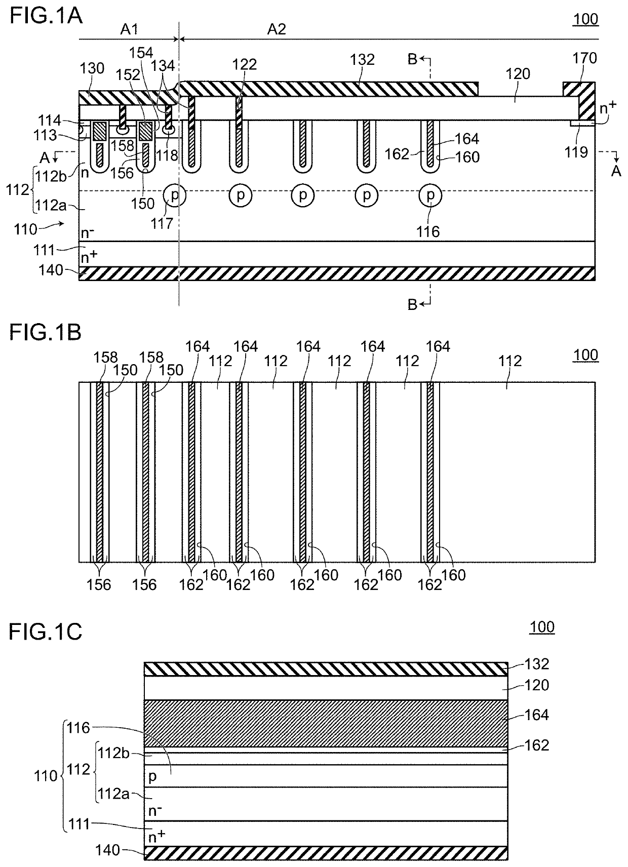
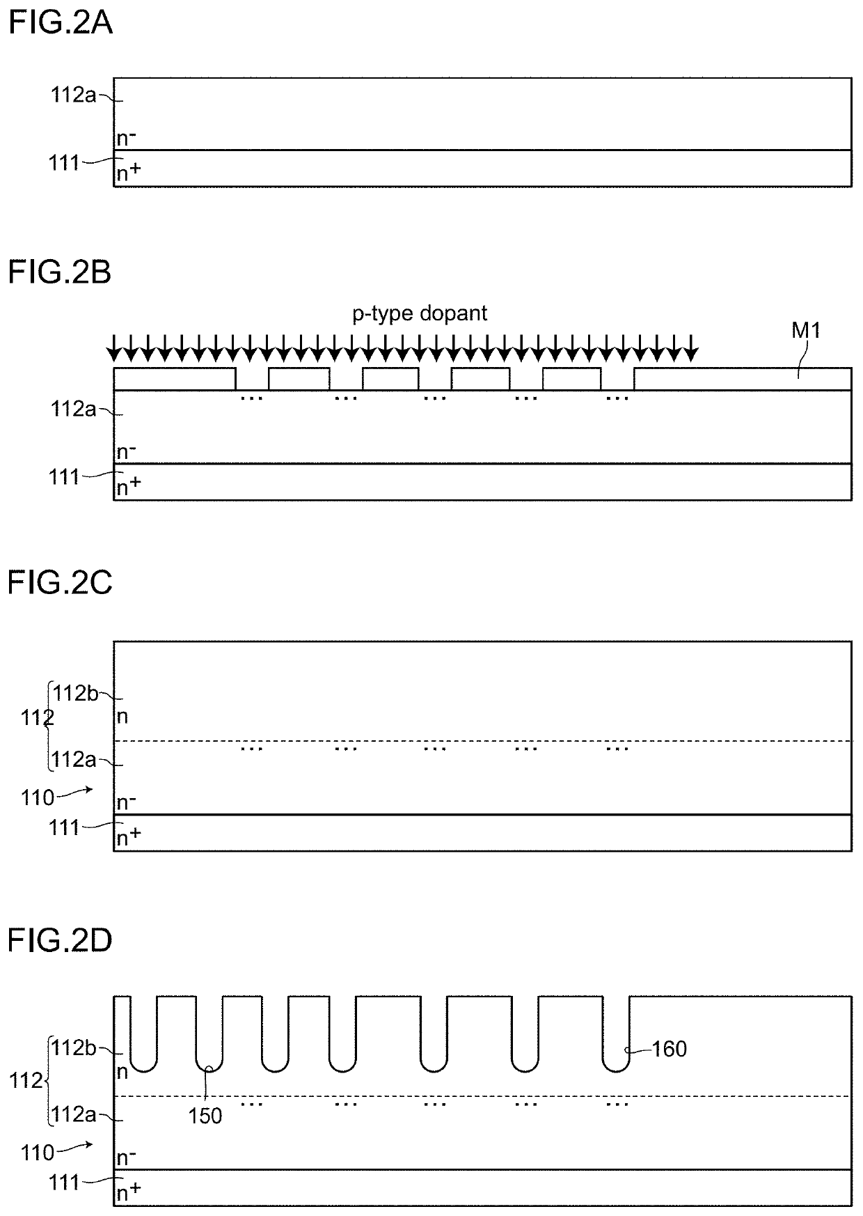
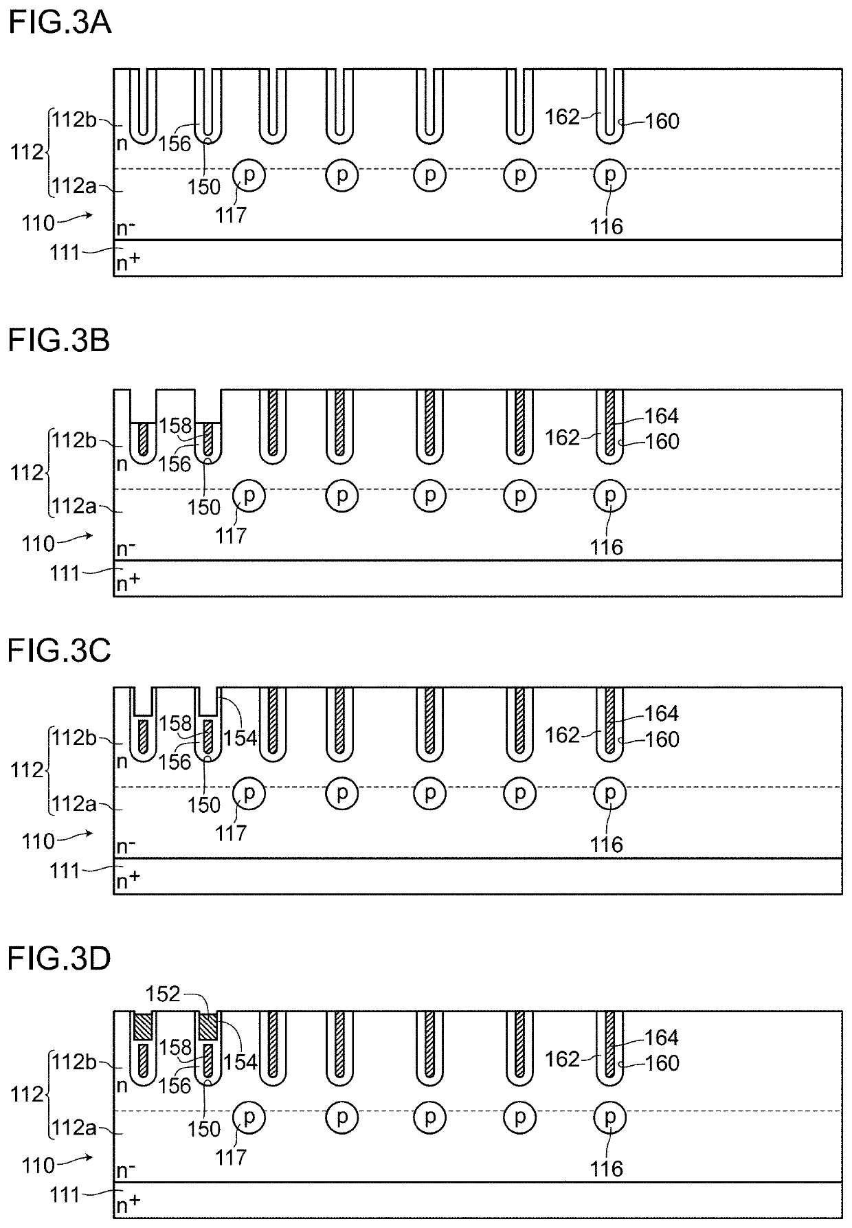
[0048]A semiconductor device 100 according to an embodiment 1 is, as shown in FIG. 1A to FIG. 1C, a semiconductor device which includes: a semiconductor base substrate 110 having a drift layer 112; a source electrode 130 (first main electrode) formed on one surface side of the semiconductor base substrate 110 by way of an interlayer insulation film 120; a drain electrode 140 (second main electrode) formed on the other surface side of the semiconductor base substrate 110, wherein an active region A1 where a main current path is formed between the source electrode 130 and the drain electrode 140 and a peripheral region A2 disposed outside the active region A1 are defined.

[0049]In the embodiment 1, the semiconductor device 100 includes: in the active region A1, a plurality of trenches 150 formed on the drift layer 112, gate electrodes 152 formed in the plurality of trenches 150 respectively by way of side walls and g...

modification 1

[0117]A semiconductor device 101 according to a modification 1 basically has substantially the same configuration as the semiconductor device 100 according to the embodiment 1. However, the semiconductor device 101 according to the modification 1 differs from the semiconductor device 100 according to the embodiment 1 with respect to the configuration of floating regions. That is, in the semiconductor device 101 according to the modification 1, as shown in FIG. 11A to FIG. 11C, each floating region 116 is disposed between peripheral trenches 160 disposed adjacently to each other.

[0118]In the same manner as the semiconductor device 100 according to the embodiment 1, in the semiconductor device 101 according to the modification 1, a semiconductor base substrate 110 includes, in a peripheral region A2, a plurality of p-type floating regions 116 which are disposed in a drift layer 112 at a depth position deeper than bottom portions of the peripheral trenches 160 in a spaced-apart manner ...

modification 2

[0119]A semiconductor device 102 according to a modification 2 basically has substantially the same configuration as the semiconductor device 100 according to the embodiment 1. However, the semiconductor device 102 according to the modification 2 differs from the semiconductor device 100 according to the embodiment 1 with respect to the configuration of floating regions. That is, in the semiconductor device 102 according to the modification 2, as shown in FIG. 12A to FIG. 12C, floating regions 116 are disposed at intermediate positions each of which is disposed between peripheral trenches 160 and just below the peripheral trenches 160.

[0120]In the semiconductor device 102 according to the modification 2, the floating regions 116 are disposed in a staggered manner such that the floating regions 116 disposed at the intermediate positions each of which is disposed between the peripheral trenches 160 are disposed on a lower stage and the floating regions disposed just below the peripher...


PUM


Abstract

A semiconductor device includes: a semiconductor base substrate including a semiconductor layer; a first main electrode; a second main electrode; a plurality of peripheral trenches formed on a surface of the semiconductor layer and having bottom portions covered by the semiconductor layer in a peripheral region; and a plurality of in-trench electrodes each embedded in each of the plurality of peripheral trenches byway of an insulation layer formed on an inner surface of the each peripheral trench, wherein the semiconductor base substrate further includes, in the peripheral region, a plurality of second conductive type floating regions disposed in the semiconductor layer at a depth position deeper than the bottom portions of the peripheral trenches in a spaced apart manner from the peripheral trenches and having a potential in a floating state.

Description

BACKGROUND OF THE INVENTION1. Field of the Invention[0001]The present invention relates to a semiconductor device and a method of manufacturing a semiconductor device.2. Description of the Related Art[0002]Conventionally, there has been known a semiconductor device where a p-type guard ring region (FLR region) and a p-type floating region are formed in a peripheral region (conventional semiconductor device 800 (see JP 2015-65238 A, for example)).[0003]As shown in FIG. 20, the conventional semiconductor device 800 includes: a semiconductor base substrate 810 having an n-type semiconductor layer 812; a source electrode 830 (first main electrode) formed on one surface side of the semiconductor base substrate 810; a drain electrode 840 (second main electrode) formed on the other surface side of the semiconductor base substrate 810. The semiconductor base substrate 810 further includes, in a peripheral region A2 outside an active region A1 where a main current path is formed between the ...

Claims


Application Information

Patent Timeline
IPC IPC(8): H01L29/06H01L29/78H01L29/40H01L29/66
CPCH01L29/407H01L29/404H01L29/7813H01L29/7811H01L29/66734H01L29/0623H01L29/78642H01L29/4236H01L29/0611H01L29/66742H01L29/0619H01L29/7397H01L29/74
Inventor TAKEMOTO, GOTAROOKUDA, TOSHIHIROKITADA, MIZUE
Owner SHINDENGEN ELECTRIC MFG CO LTD
Why Eureka
Try Eureka