

Method of manufacturing mos-type semiconductor device
- Summary
- Abstract
- Description
- Claims
- Application Information
AI Technical Summary
Benefits of technology
Problems solved by technology
Method used
Image

Examples
example 1
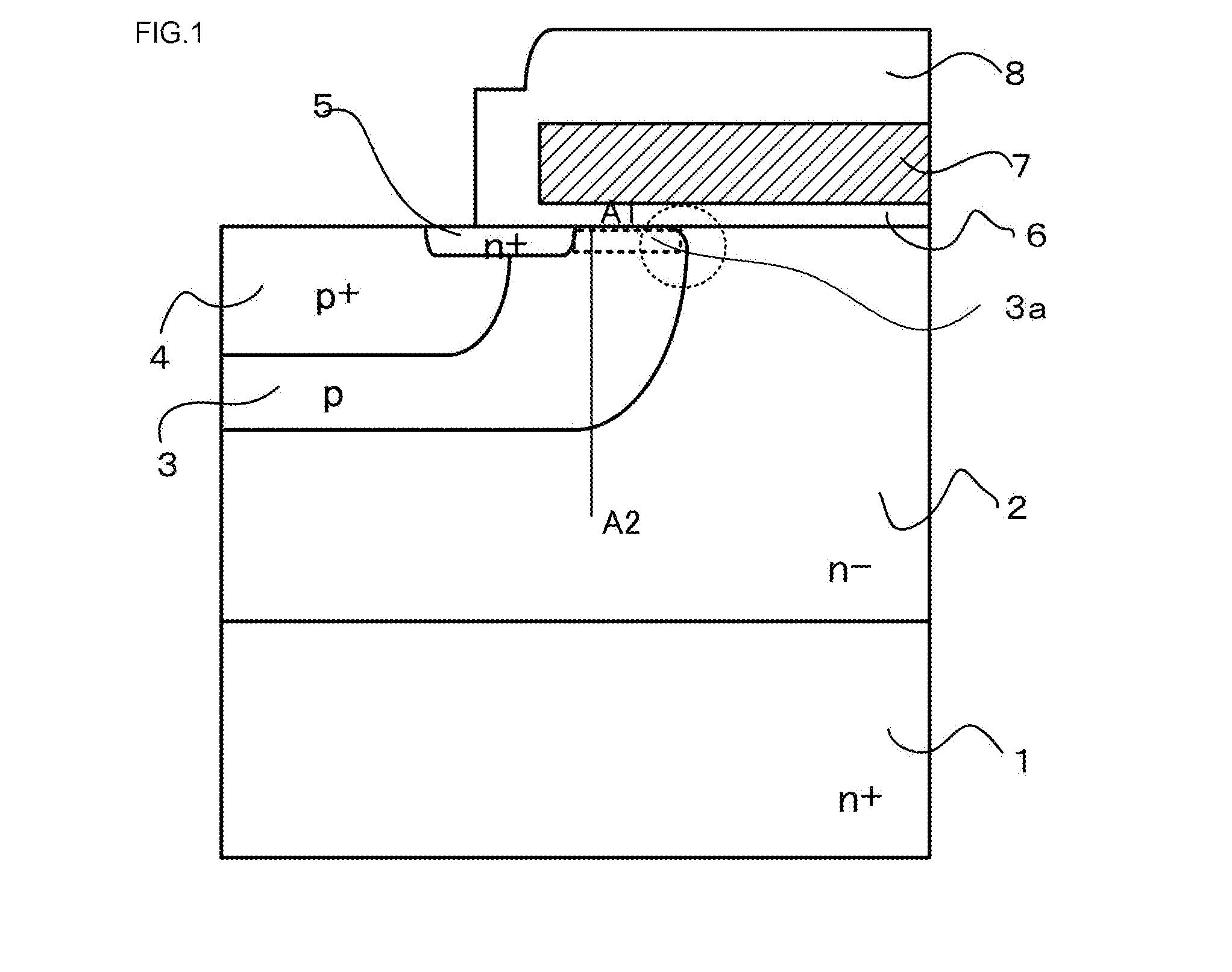
[0059]FIG. 1 illustrates a cross-sectional view of a main portion including a surface MOS structure of a power MOSFET which is one of MOS-type semiconductor devices according to the present invention. FIGS. 3 to 10 are cross-sectional views of a main portion of a semiconductor substrate, illustrating the steps of manufacturing an n-channel MOSFET as one example of a method of manufacturing a MOS-type semiconductor device according to the present invention. FIG. 19 is a flowchart illustrating the steps of the manufacturing method according to the present invention.
[0060]A thick field oxide film 11 is thermally oxidized so as to grow on a surface of a silicon semiconductor substrate. The silicon semiconductor substrate is a stacked layer including an n+-type low-resistance semiconductor substrate 1 and an n−-type drift layer 2. Photolithography and oxide film etching is performed to form an oxide film mask having an opening pattern for forming a p-type well region. Up to now, an oxide...
example 2
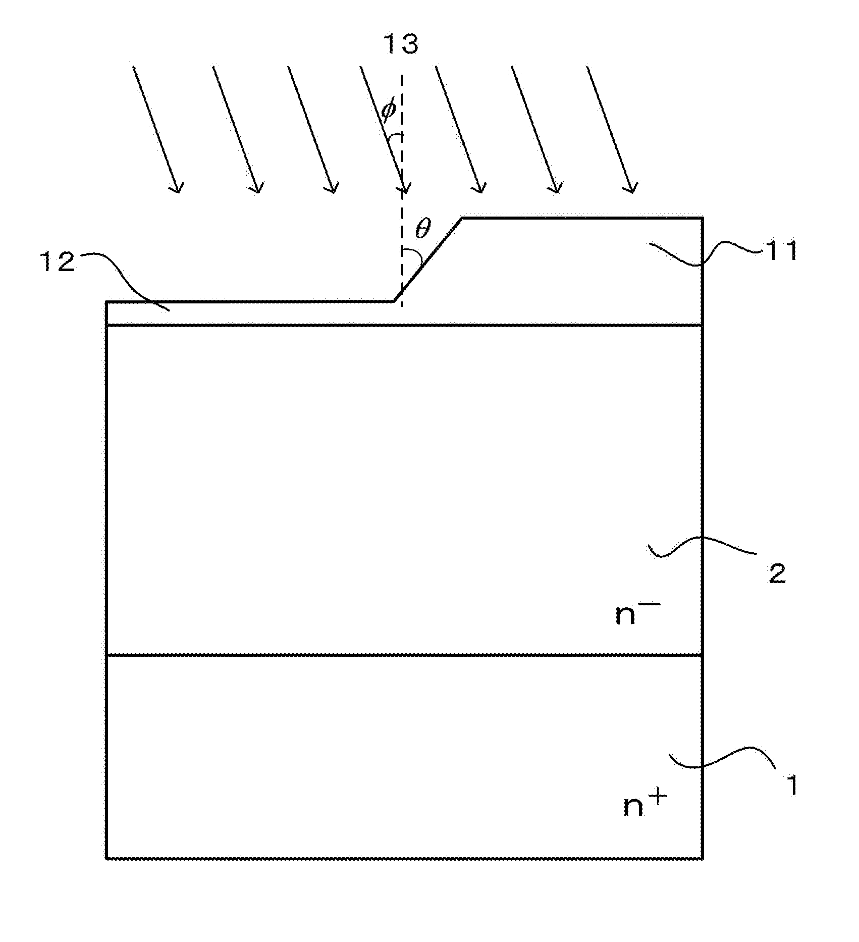
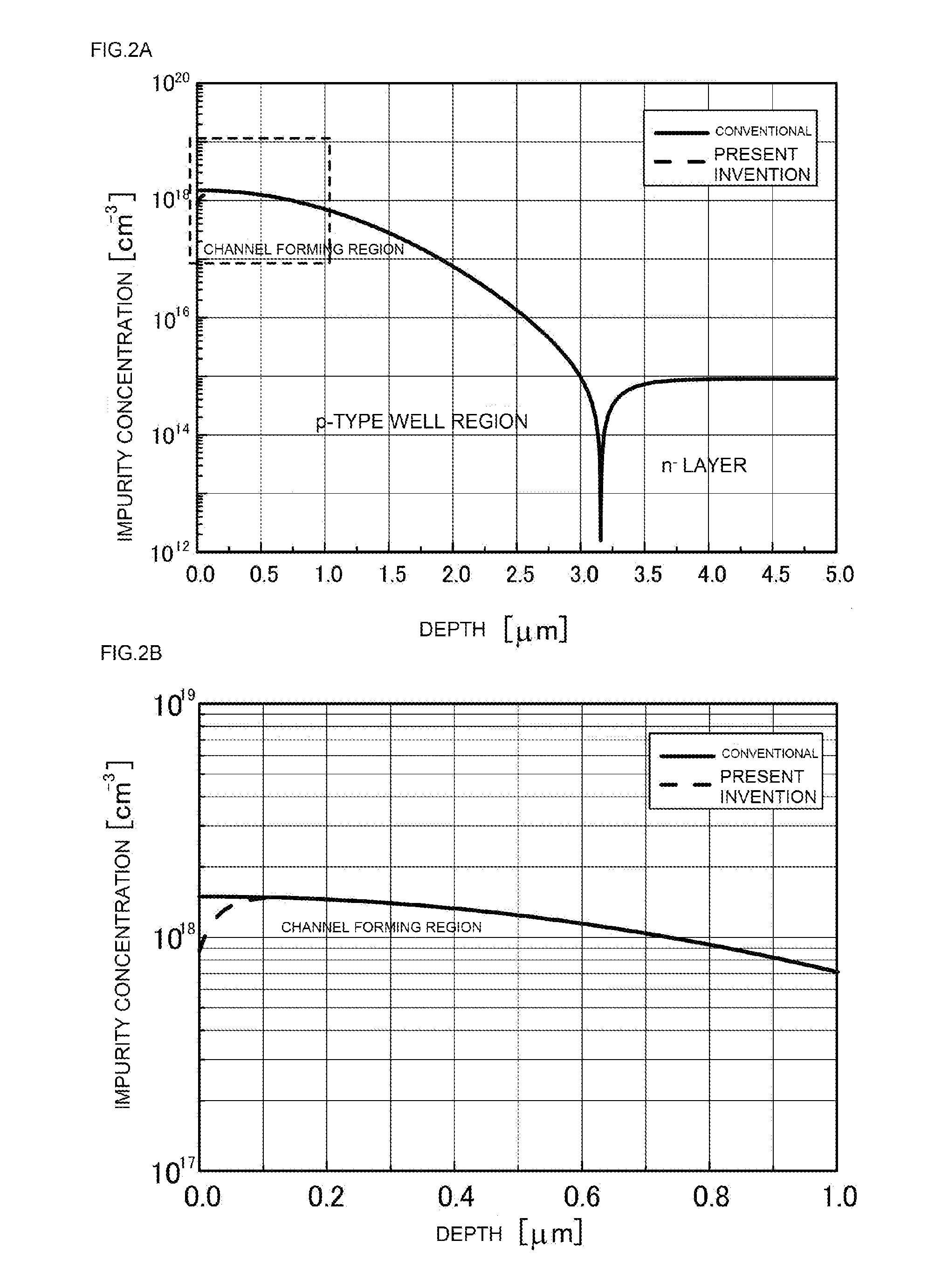
[0076]In the method of Example 1, when a MOSFET having a very small cell pattern having such a small channel length as described above is manufactured, there is a problem in that the junction terminal of the p-type well region 3 has such a roll-in shape as shown in FIG. 10 and a short-channel effect is likely to occur. In Example 2, when a MOSFET having a very small cell pattern is manufactured, etching is performed so that a tapered portion is formed in an edge close to the opening, of the oxide film mask used for the self-alignment, which is different from the MOSFET of Example 1.
[0077]Hereinafter, a method of manufacturing a MOSFET according to Example 2 will be described. The flow of major steps is the same as that of FIG. 19 described in Example 1.
[0078]First, a thick field oxide film 11 is grown on a surface of a silicon semiconductor substrate which is a stacked layer including an n+-type low-resistance semiconductor substrate 1 and an n−-type drift layer 2. Photolithography ...
PUM
 Abstract
Description
Claims
Application Information