Vertical extended cavity surface emission laser and method for manufacturing a light emitting component of the same

Active Publication Date: 2010-08-05
KONINKLIJKE PHILIPS ELECTRONICS NV
View PDF10 Cites 81 Cited by
  • Summary
  • Abstract
  • Description
  • Claims
  • Application Information

AI Technical Summary

Benefits of technology

[0027]In a further preferred embodiment the metallization layer is arranged in a node of a standing wave of the laser radiation formed inside of the laser cavity. In this position the metallization layer doe

Problems solved by technology

The thermal conductivity of transparent substrates however is not sufficient to use them as an effective heat sink.
Furthermore, a homo

Method used


Image

  • Vertical extended cavity surface emission laser and method for manufacturing a light emitting component of the same
  • Vertical extended cavity surface emission laser and method for manufacturing a light emitting component of the same
  • Vertical extended cavity surface emission laser and method for manufacturing a light emitting component of the same

Examples


Example

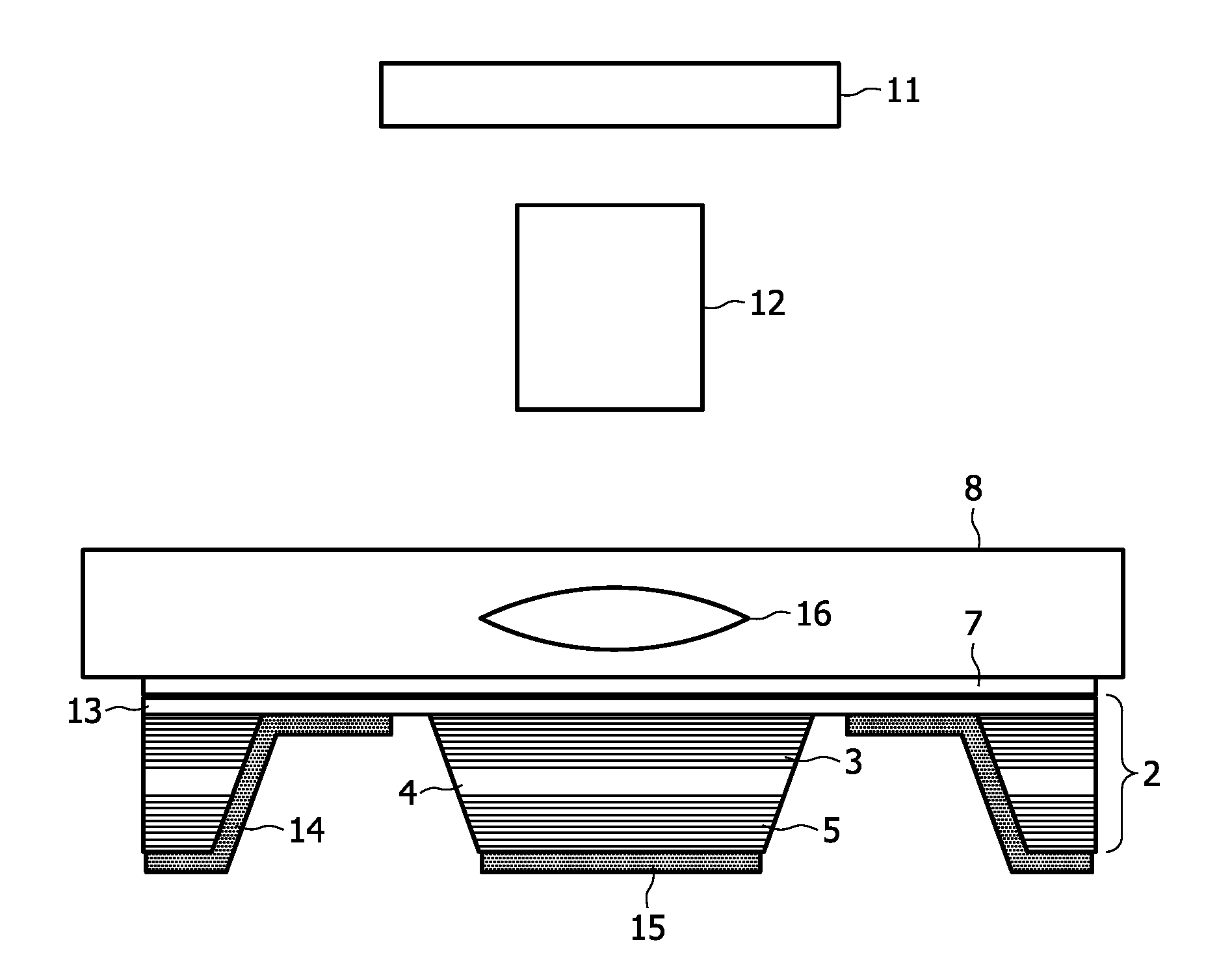
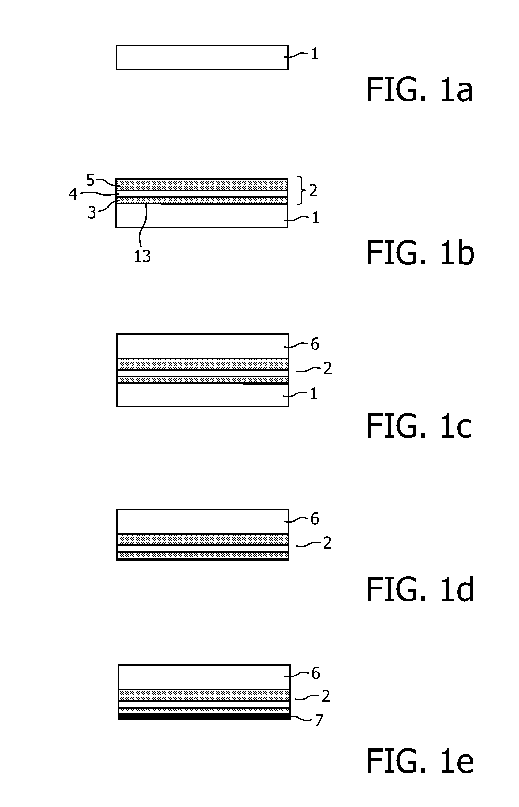
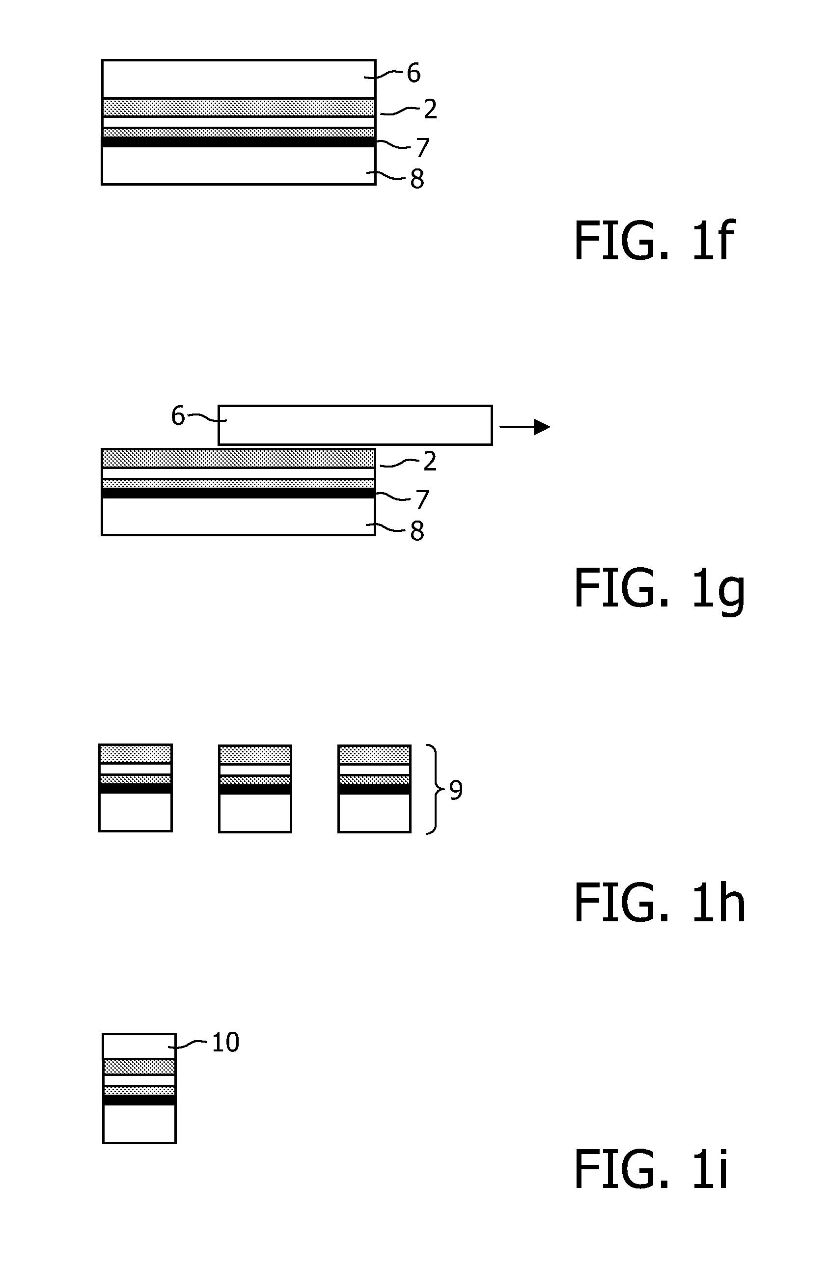
[0036]FIG. 1 shows a sequence of method steps which are performed according to an exemplary embodiment of the proposed method. In a first step, according to FIG. 1a, a GaAs semiconductor substrate 1 is provided. A layer stack 2 forming a p-doped current injection layer 13, a lower distributed Bragg reflector 3, an active region 4 and an upper distributed Bragg reflector 5 is epitaxially grown on the semiconductor substrate 1 (FIG. 1b). The two DBRs 3, 5 are stacks of many pairs of semiconductor layers, in the most simple case each λ / 4 thick at the design wavelength λ, i.e. the wavelength of the laser in the semiconductor material. Each pair is composed of a high and low refractive index layer, for example of AlGaAs. The upper DBR 5 is designed to have a reflectance of 98-99.9% (or even >99.9%) at the laser wavelength and is therefore formed of more than 20 p-doped layer pairs. In the case of the lower DBR 3, this DBR is formed of only between 4 to 13 pairs of n-doped layers resultin...


PUM


Abstract

The present invention relates to a method of manufacturing the light emitting component of a VECSEL and the corresponding VECSEL. In the method a layer stack (2) is epitaxially grown on a semiconductor substrate (1). The layer stack comprises an active region (4), an upper distributed Bragg reflector (5) and a n- or p-doped current injection layer (13) arranged between the active region (4) and the semiconductor substrate (1). A mechanical support (6) or submount is bonded to an upper side of the layer stack (2) and the semiconductor substrate (1) is subsequently removed. A metallization layer (7) is optionally deposited on the lower side of the layer stack (2) and an optically transparent substrate (8) is bonded to this lower side. The proposed method allows the manufacturing of such a component in a standard manner and results in a VECSEL with a homogenous current injection and high efficiency of heat dissipation.

Description

FIELD OF THE INVENTION[0001]The present invention relates to a vertical extended cavity surface emission laser (VECSEL) comprising an extended mirror forming a first end mirror of the extended cavity, a layer stack having at least an active region for light emission and a distributed Bragg reflector (DBR) forming the second end mirror of said extended cavity, and a substrate to which the layer stack is attached. The invention also refers to a method of manufacturing a light emitting component of such a vertical extended cavity surface emission laser.[0002]Vertical extended cavity surface emitting lasers are a promising technology for projection applications. The IR emitting components of such a laser can be converted to blue, green and red light by second harmonic generation with nonlinear crystals inside the extended laser cavity.BACKGROUND OF THE INVENTION[0003]Vertical cavity surface emitting lasers (VCSEL) are typically formed of a layer stack comprising an active (gain) region,...

Claims


Application Information

Patent Timeline
IPC IPC(8): H01S5/14H01L33/48H01L33/60H01S5/183H01S5/02
CPCH01S3/109H01S5/0215H01S5/0217H01S5/18305H01S5/024H01S5/0425H01S5/14H01S5/02272H01S5/04257H01S5/0237
Inventor MOENCH, HOLGERVALSTER, ADRIAANGRABHERR, MARTIN
Owner KONINKLIJKE PHILIPS ELECTRONICS NV
Why Eureka
Try Eureka