

Transistor and method for operating the same
a transistor and channel current technology, applied in the field of transistors, can solve the problems of difficult to raise the gate voltage, difficult to increase the drain current in sufficient amounts, and difficulty in fet to exhibit enhancement-type (normally off-type) characteristics, etc., to achieve large operating current, increase the channel current, and promote electron generation.
- Summary
- Abstract
- Description
- Claims
- Application Information
AI Technical Summary
Benefits of technology
Problems solved by technology
Method used
Image

Examples
first embodiment
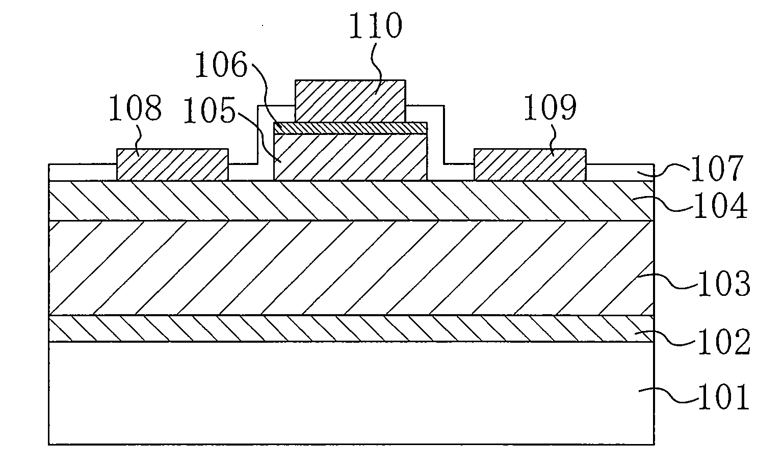
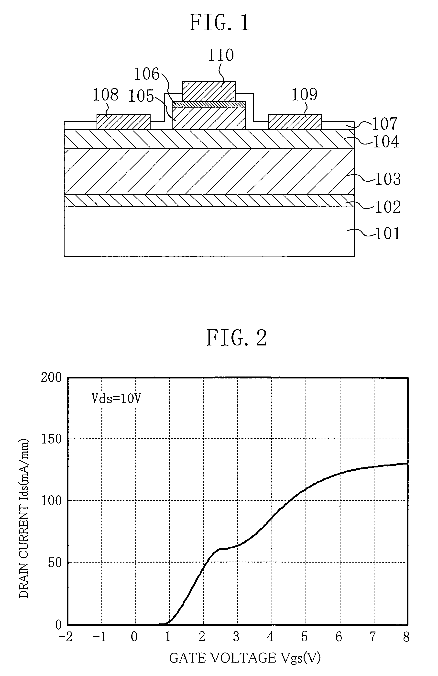
[0054]FIG. 1 is a sectional view showing a nitride semiconductor device according to a first embodiment of the present invention.
[0055]Referring to FIG. 1, the nitride semiconductor device according to the first embodiment includes a sapphire substrate 101, an AlN buffer layer 102, an undoped GaN layer 103, an undoped AlGaN layer 104, a p-type control layer 105, and a p-type contact layer 106. The sapphire substrate 101 has the (0001) plane as a principal plane. The AlN buffer layer 102 is provided on the (0001) plane of the sapphire substrate 101. The undoped GaN layer 103 is provided on the AlN buffer layer 102. The undoped AlGaN layer 104 is provided on the undoped GaN layer 103. The p-type control layer 105 is provided on a portion of the undoped AlGaN layer 104, and made of AlGaN containing p-type impurities. The p-type contact layer 106 is provided on the p-type control layer 105, and made of GaN containing p-type impurities with a higher concentration than those in the p-type...
second embodiment
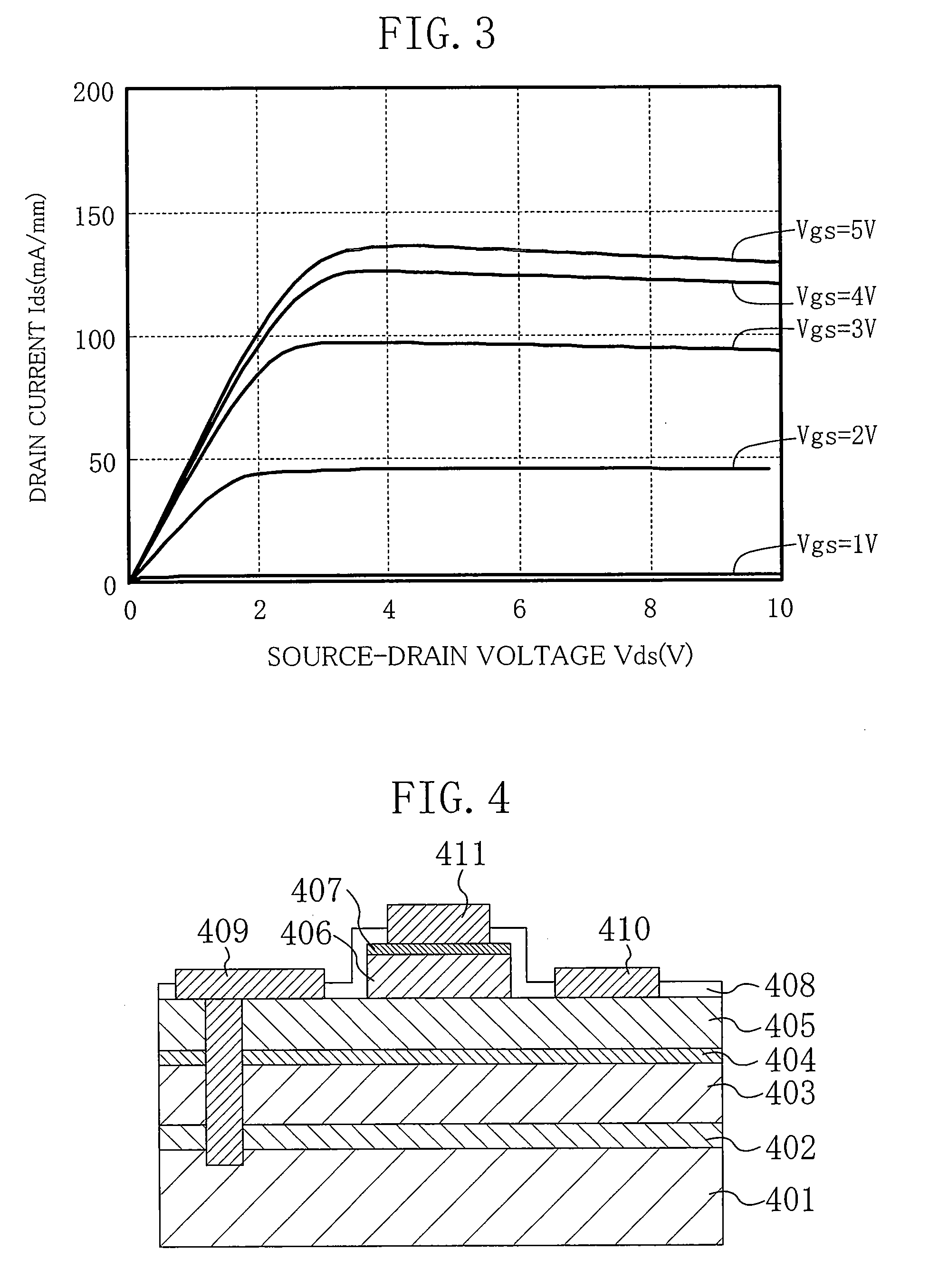
[0077]FIG. 4 is a sectional view showing a nitride semiconductor device according to a second embodiment of the present invention.
[0078]Referring to FIG. 4, the nitride semiconductor device according to the second embodiment includes an n-type Si substrate 401, an AlN buffer layer 402, an underlying undoped AlGaN layer 403, an undoped GaN layer 404, an undoped AlGaN layer 405, a p-type control layer 406, and a p-type contact layer 407. The n-type Si substrate 401 has the (111) plane as a principal plane. The AlN buffer layer 402 is provided on the (111) plane of the n-type Si substrate 401. The underlying undoped AlGaN layer 403 is provided on the AlN buffer layer 402. The undoped GaN layer 404 is provided on the underlying undoped AlGaN layer 403. The undoped AlGaN layer 405 is provided on the undoped GaN layer 404. The p-type control layer 406 is provided on a portion of the undoped AlGaN layer 405, and made of AlGaN containing p-type impurities. The p-type contact layer 407 is pr...
third embodiment
[0088]FIG. 7 is a sectional view showing a nitride semiconductor device according to a third embodiment of the present invention.
[0089]Referring to FIG. 7, the nitride semiconductor device according to the third embodiment includes a sapphire substrate 701, an AlN buffer layer 702, an undoped GaN layer 703, an undoped AlGaN layer 704, a lightly doped p-type control layer 705, a heavily doped p-type control layer 706, and a p-type contact layer 707. The sapphire substrate 701 has the (0001) plane as a principal plane. The AlN buffer layer 702 is provided on the (0001) plane of the sapphire substrate 701. The undoped GaN layer 703 is provided on the AlN buffer layer 702. The undoped AlGaN layer 704 is provided on the undoped GaN layer 703. The lightly doped p-type control layer 705 is provided on a portion of the undoped AlGaN layer 704, and made of AlGaN containing p-type impurities. The heavily doped p-type control layer 706 is provided on the lightly doped p-type control layer 705,...
PUM
 Abstract
Description
Claims
Application Information