Trench gate charge storage type IGBT and manufacturing method thereof

A technology of charge storage and charge storage layer, which is applied in the manufacture of circuits, electrical components, semiconductor/solid-state devices, etc., and can solve problems such as increased switching loss, reduced device switching speed, and increased device switching loss

Active Publication Date: 2018-08-28
UNIV OF ELECTRONIC SCI & TECH OF CHINA
View PDF7 Cites 9 Cited by
  • Summary
  • Abstract
  • Description
  • Claims
  • Application Information

AI Technical Summary

Problems solved by technology

[0006] The implementation of method (1) will increase the gate-emitter capacitance and gate-collector capacitance at the same time, and the switching process of the IGBT is essentially the process of charging/discharging the gate capacitance, so the increase in the gate capacitance will Makes the charging/discharging time longer, which in turn causes the switching speed to decrease
Therefore, the deep trench gate depth will reduce the switching speed of the device, increase the switching loss of the device, and affect the compromise characteristics of the device's conduction voltage drop and switching loss; and the implementation of method (2) will increase the device's switching loss The gate capacitance will reduce the switching speed of the device and increase the switching loss, which will affect the compromise be

Method used


Image

  • Trench gate charge storage type IGBT and manufacturing method thereof
  • Trench gate charge storage type IGBT and manufacturing method thereof
  • Trench gate charge storage type IGBT and manufacturing method thereof

Examples


Embodiment 1

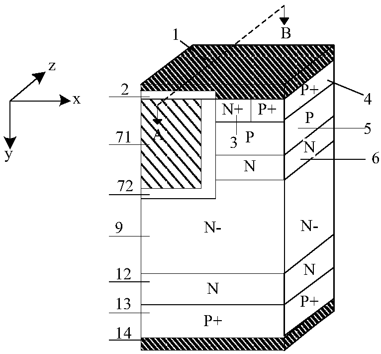
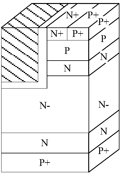
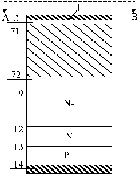
[0099] The present invention provides a trench gate charge storage type IGBT, one quarter of the cell is as Figure 4 As shown, the section along AB line and A'B' line is as follows Figure 6 and Figure 7 As shown, a three-dimensional coordinate system is established with any inflection point of the quarter cell as the origin, and the bottom surface of the quarter cell intersects with the two sides of the inflection point as the x-axis and z-axis respectively, passing through the inflection point and A straight line perpendicular to the bottom surface is used as the y-axis, and the directions of the x, y, and z-axes refer to Figure 4 ;

[0100] The quarter cell includes: a collector metal 14, a P-type collector region 13, an N-type field stop layer 12, an N-type drift region 9, and an emitter metal 1 stacked sequentially from bottom to top; The top layer of the N-type drift region 9 has an N-type charge storage layer 6, a P-type base region 5, a P+ emission region 4 and a...

Embodiment 2

[0103] The present invention provides a trench gate charge storage type IGBT, one quarter of the cell is as Figure 8 As shown, the section along AB line and A'B' line is as follows Figure 10 and Figure 11 As shown, a three-dimensional coordinate system is established with any inflection point of the quarter cell as the origin, and the bottom surface of the quarter cell intersects with the two sides of the inflection point as the x-axis and z-axis respectively, passing through the inflection point and A straight line perpendicular to the bottom surface is used as the y-axis, and the directions of the x, y, and z-axes refer to Figure 8 ;

[0104] Compared with Example 1, the difference of this implementation is that: the P-type layer 10 is introduced at the bottom of the shielding trench structure, and the P-type layer 10 and the shielding electrode 81 are connected through the shielding electrode dielectric layer 82, and other structures All are the same as in Embodiment...

Embodiment 3

[0106] The present invention provides a trench gate charge storage type IGBT, one quarter of the cell is as Figure 12 As shown, the section along AB line and A'B' line is as follows Figure 14 and Figure 15 As shown, a three-dimensional coordinate system is established with any inflection point of the quarter cell as the origin, and the bottom surface of the quarter cell intersects with the two sides of the inflection point as the x-axis and z-axis respectively, passing through the inflection point and A straight line perpendicular to the bottom surface is used as the y-axis, and the directions of the x, y, and z-axes refer to Figure 12 ;

[0107] Compared with Embodiment 2, the difference of this implementation is that the side wall gate electrode 71 extends from one end of the device to the other end along the z-axis, that is, the upper half of the shielding trench structure is cut off by the trench gate structure along the z-axis direction, Except that other structure...


PUM

PropertyMeasurementUnit
Thicknessaaaaaaaaaa
Thicknessaaaaaaaaaa

Abstract

The invention discloses a trench gate charge storage type IGBT, and belongs to the technical field of semiconductor power devices. A conventional trench gate structure is widened, and a side wall gateelectrode structure is employed for forming a mesa structure located below a base region. moreover, a shielding trench structure for shielding the electric field of a charge storage layer is introduced, thereby improving the carrier injection enhancement effect, and improving the compromise between a forwarding ON voltage drop Vceon and the OFF loss Eoff. The electric field concentration effect at the tip of the bottom of a trench is alleviated, and the breakdown voltage of a device is effectively improved. The gate capacitance of the device, especially the Miller capacitance CGC and the gatecharge QG, is reduced, the switching speed of the device is improved, the switching loss of the device is reduced, and the requirements for the capability of a gate drive circuit are reduced. The constraint on the doping concentration of an N-type charge storage layer and the withstand voltage of the device from the thickness are avoided, the saturation current density is reduced, and a short-circuit safe operating region (SCSOA) of the device is improved. Moreover, an EMI effect is effectively inhibited when the device is turned on. In addition, the manufacturing method is compatible with aconventional trench gate charge storage type IGBT manufacturing method.

Description

technical field [0001] The invention belongs to the technical field of power semiconductor devices, in particular to a trench gate charge storage type insulated gate bipolar transistor (CSTBT). Background technique [0002] Insulated Gate Bipolar Transistor (IGBT) was proposed on the basis of research on power MOSFET, BJT and SCR / GTO, etc. In the late 1970s and early 1980s, it was invented by introducing a PN junction into the back substrate of the power MOSFET structure and achieve mass production. The conductance modulation effect introduced by the PN junction on the back of the device when the device is turned on makes the IGBT a new type of power electronic device that is composed of a MOS field effect transistor and a bipolar junction transistor (BJT), and can also be equivalent to a bipolar junction transistor (BJT). ) driven MOSFET structure. IGBT combines the characteristics of both MOSFET and BJT: not only has the advantages of high input impedance, low control po...

Claims


Application Information

Patent Timeline
IPC IPC(8): H01L29/40H01L29/423H01L29/739H01L21/331H01L21/28
CPCH01L29/407H01L29/4236H01L29/66348H01L29/7397H01L29/7398
Inventor 张金平赵倩王康刘竞秀李泽宏张波
Owner UNIV OF ELECTRONIC SCI & TECH OF CHINA
Why Eureka
Try Eureka