Display device, display module, and electronic device

a display module and electronic device technology, applied in the field of display devices, can solve the problems of increasing the resistance of the gate electrode, the gate capacitance of such a transistor, and the electric field of the gate electrode is excessively increased, so as to achieve high field-effect mobility, high reliability, and high field-effect mobility

Active Publication Date: 2017-06-29
SEMICON ENERGY LAB CO LTD
View PDF2 Cites 11 Cited by
  • Summary
  • Abstract
  • Description
  • Claims
  • Application Information

AI Technical Summary

Benefits of technology

[0010]Transistors including oxide layers are expected to be used for display devices. Such transistors are required to have high field-effect mobility and high reliability. To achieve high field-effect mobility, it is effective in a transistor to electrically surround an oxide layer where a channel is formed. However, there is a problem in that the gate capacitance of such a transistor in which an oxide layer where a channel is formed is electrically surrounded by electric fields of gate electrodes is excessively increased when the transistor is driven with a signal of a scan line.

Problems solved by technology

However, there is a problem in that the gate capacitance of such a transistor in which an oxide layer where a channel is formed is electrically surrounded by electric fields of gate electrodes is excessively increased when the transistor is driven with a signal of a scan line.
However, the use of a gate electrode that is formed with, for example, an oxide layer and releases oxygen by being heated as a top gate to achieve high reliability causes a problem of increasing the resistance of the gate electrode, or the resistance of a scan line, compared with the use of a gate electrode formed with metal.
However, such a structure has a problem in that forming an opening for connecting a top gate and a bottom gate in a small region such as a pixel region makes the layout difficult, resulting in difficulty in fabricating a high-definition display device.
Although a metal wiring can be stacked over a gate electrode that releases oxygen by being heated so that the resistance of a scan line is reduced, this structure has a problem in that the number of steps increases and thus the manufacturing cost increases.

Method used


Image

  • Display device, display module, and electronic device
  • Display device, display module, and electronic device
  • Display device, display module, and electronic device

Examples


embodiment 1

[0058]In this embodiment, a configuration example of a display device of one embodiment of the present invention will be described.

Configuration Example of Circuit Diagram

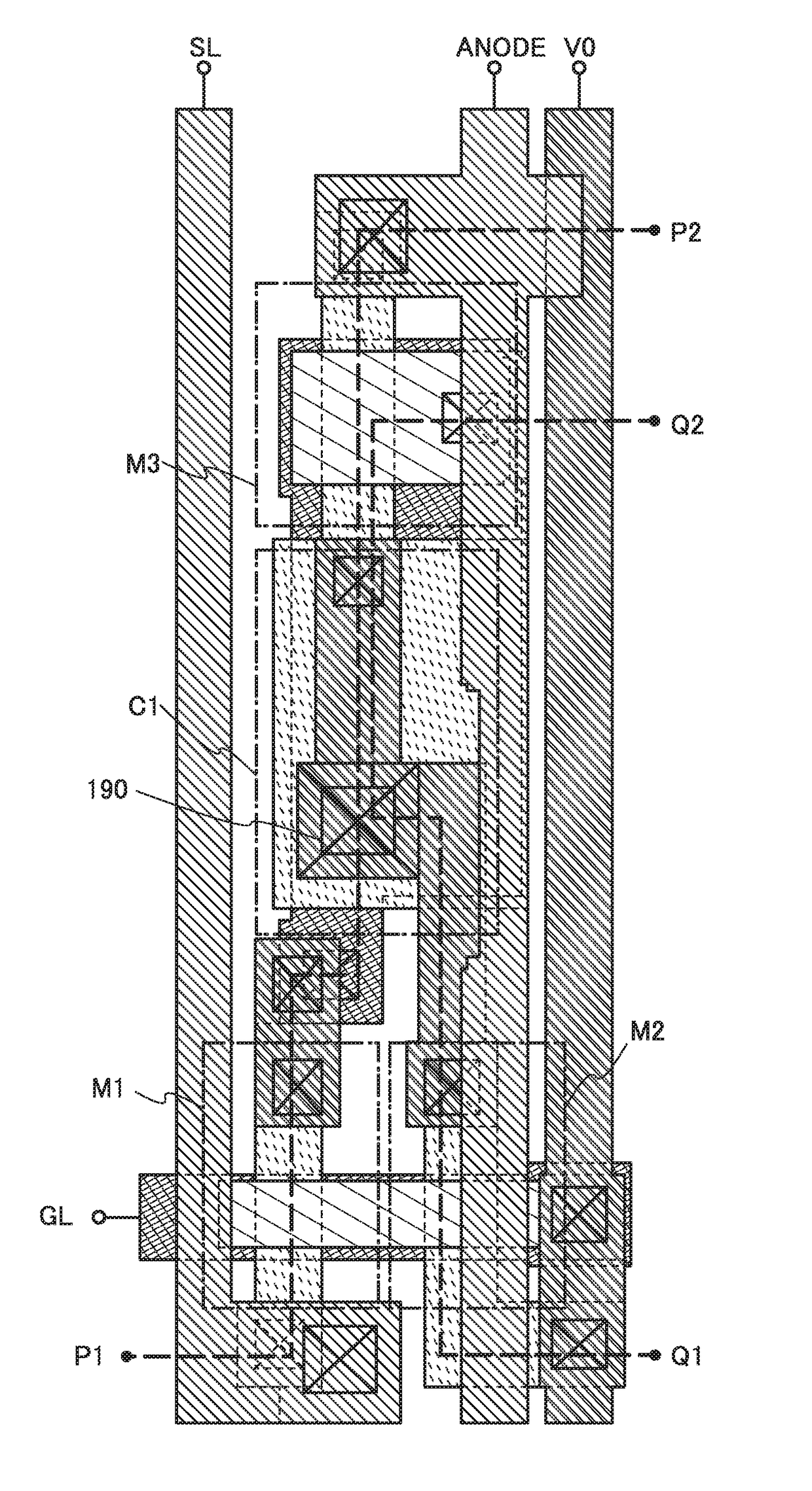
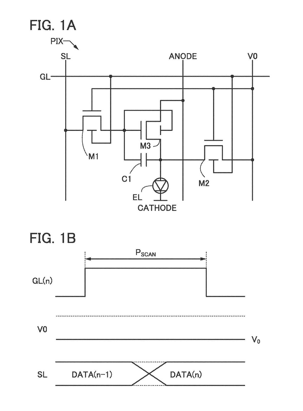
[0059]FIG. 1A is a circuit diagram of a pixel included in a display device.

[0060]A pixel PIX includes a transistor M1, a transistor M2, a transistor M3, a capacitor C1, and a light-emitting element EL. The pixel PIX is connected to a scan line GL, a signal line SL, a current supply line ANODE, a wiring V0, and a common wiring CATHODE. The pixel PIX corresponds to a subpixel included in a pixel that performs color display. Although description will be given assuming that the transistors M1 to M3 are n-channel transistors, the transistors M1 to M3 may be p-channel transistors.

[0061]The scan line GL is a wiring for supplying a scan signal to a pixel. A scan signal is a signal for controlling the conduction state of a transistor that is supplied with the scan signal. The signal line SL is a wiring for supplying a signa...

embodiment 2

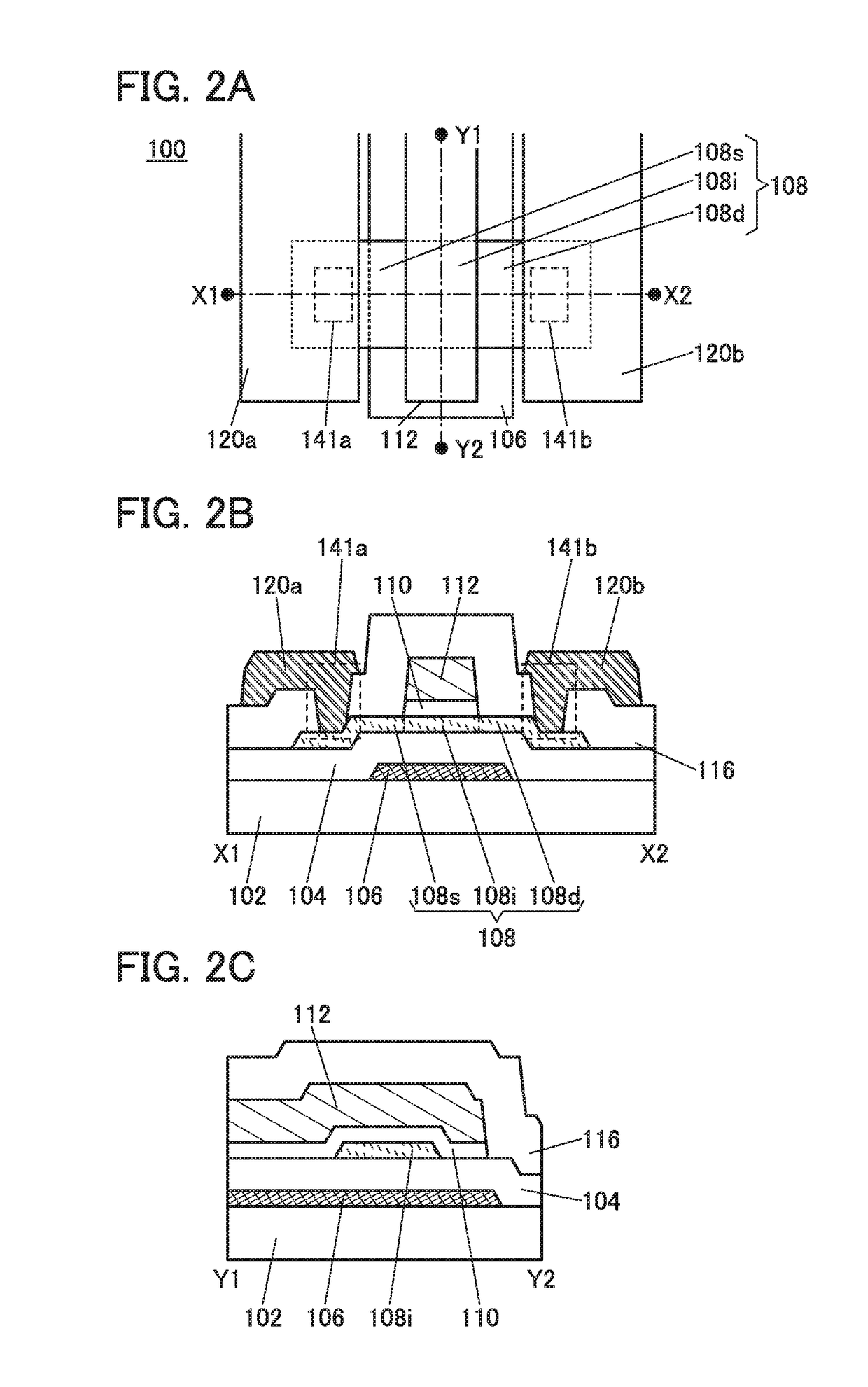
[0143]In this embodiment, an example of a cross-sectional structure of a display device of one embodiment of the present invention will be described.

Structure Example of Display Device

[0144]FIG. 9 is a schematic top view of a display device 10 described below. The display device 10 includes a pixel portion 11, a scan line driver circuit 12, a signal line driver circuit 13, a terminal portion 15, a plurality of wirings 16a, a plurality of wirings 16b, and the like.

Cross-Sectional Structure Example 1-1

[0145]FIG. 10 is a schematic cross-sectional view of the display device 10. FIG. 10 shows a cross section taken along the section line A1-A2 of FIG. 9.

[0146]The display device 10 includes a first substrate 201 and a second substrate 202 which are bonded to each other with a bonding layer 220.

[0147]The terminal portion 15, the wiring 16b; a transistor 255 that is included in the signal line driver circuit 13, transistors 251 and 252, a capacitor 253, and a light-emitting element 254 that ...

modification example

[0175]An example of a touch panel including a touch sensor will be described below.

[0176]FIG. 12 shows an example of a touch panel in which an on-cell touch sensor is used in the structure shown as an example in FIG. 10.

[0177]Over the second substrate 202, a conductive layer 291 and a conductive layer 292 are covered with an insulating layer 294. A conductive layer 293 is provided over the insulating layer 294. The conductive layer 293 is electrically connected, through an opening of the insulating layer 294, to two conductive layers 292 between which the conductive layer 291 is provided. The insulating layer 294 is bonded to a substrate 296 with a bonding layer 295.

[0178]The amount of the capacitance formed between the conductive layers 291 and 292 changes with the approach of an object, so that the approach or contact of the object can be sensed. A lattice arrangement of the plurality of conductive layers 291 and the plurality of conductive layers 292 allows location information t...


PUM


Abstract

A novel display device or the like in which a transistor connected to a scan line has small gate capacitance is provided. A novel display device or the like in which a scan line has low resistance is provided. A novel display device or the like in which pixels can be arranged with high density is provided. A novel display device or the like that can be manufactured without an increase in cost is provided. In a transistor including a first gate electrode and a second gate electrode, the first gate electrode is formed using a metal material with low resistance and the second gate electrode is formed using a metal oxide material that can reduce oxygen vacancies in an oxide semiconductor layer. The first gate electrode is connected to the scan line, and the second gate electrode is connected to a wiring to which a constant potential is supplied.

Description

TECHNICAL FIELD[0001]One embodiment of the present invention relates to a display device provided with a transistor including an oxide semiconductor.[0002]Note that one embodiment of the present invention is not limited to the above technical field. The technical field of one embodiment of the invention disclosed in this specification and the like relates to an object, a method, or a manufacturing method. One embodiment of the present invention relates to a process, a machine, manufacture, or a composition of matter. In particular, one embodiment of the present invention relates to a semiconductor device, a display device, a light-emitting device, a power storage device, a storage device, a driving method thereof, or a manufacturing method thereof.BACKGROUND ART[0003]A technique for forming a transistor using a semiconductor layer formed over a substrate having an insulating surface (also referred to as a field-effect transistor (FET) or a thin film transistor (TFT)) has been attrac...

Claims


Application Information

Patent Timeline
Patent Type & Authority Applications(United States)
IPC IPC(8): H01L27/12H01L29/786H01L29/49H01L29/04
CPCH01L27/1225H01L29/045H01L29/7869H01L27/3262H01L29/4908H01L29/78648H01L27/124G09G3/32G09G3/3225H01L27/1255G09G2300/04G09G2300/0426H01L27/1266H10K59/126H10K59/1213
Inventor TOYOTAKA, KOUHEITAKAHASHI, KEISHISHIDO, HIDEAKIKUSUNOKI, KOJI
Owner SEMICON ENERGY LAB CO LTD
Why Eureka
Try Eureka