Thin film transistor

Active Publication Date: 2010-09-30
SEMICON ENERGY LAB CO LTD
View PDF18 Cites 26 Cited by
  • Summary
  • Abstract
  • Description
  • Claims
  • Application Information

AI Technical Summary

Benefits of technology

[0009]An object of one embodiment of the present invention is to provide a TFT in which on current is larger and field-effect mobility is higher than those of the conventional TFTs.
[0010]Another embodiment of the present invention is

Problems solved by technology

That is, current drive capability is low.
Thus, there is a problem in that, when a protection circuit is formed using a TFT including an amorphous semiconductor film, a large-sized transistor should be formed as a countermeasure against electrostatic breakdown, which leads to hindrance to narrower frame parts.
Further, there is also another problem in that parasitic capacitance between a scan line electrically connected to a gate electrode and a signal line electrically connected to a source electrode or a drain electrode may be increa

Method used


Image

  • Thin film transistor
  • Thin film transistor
  • Thin film transistor

Examples


embodiment 1

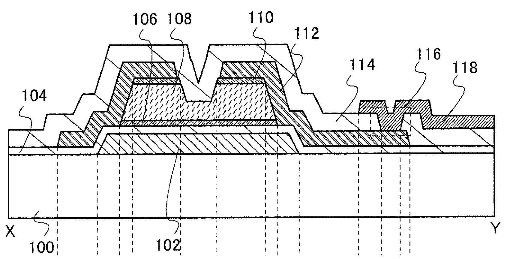
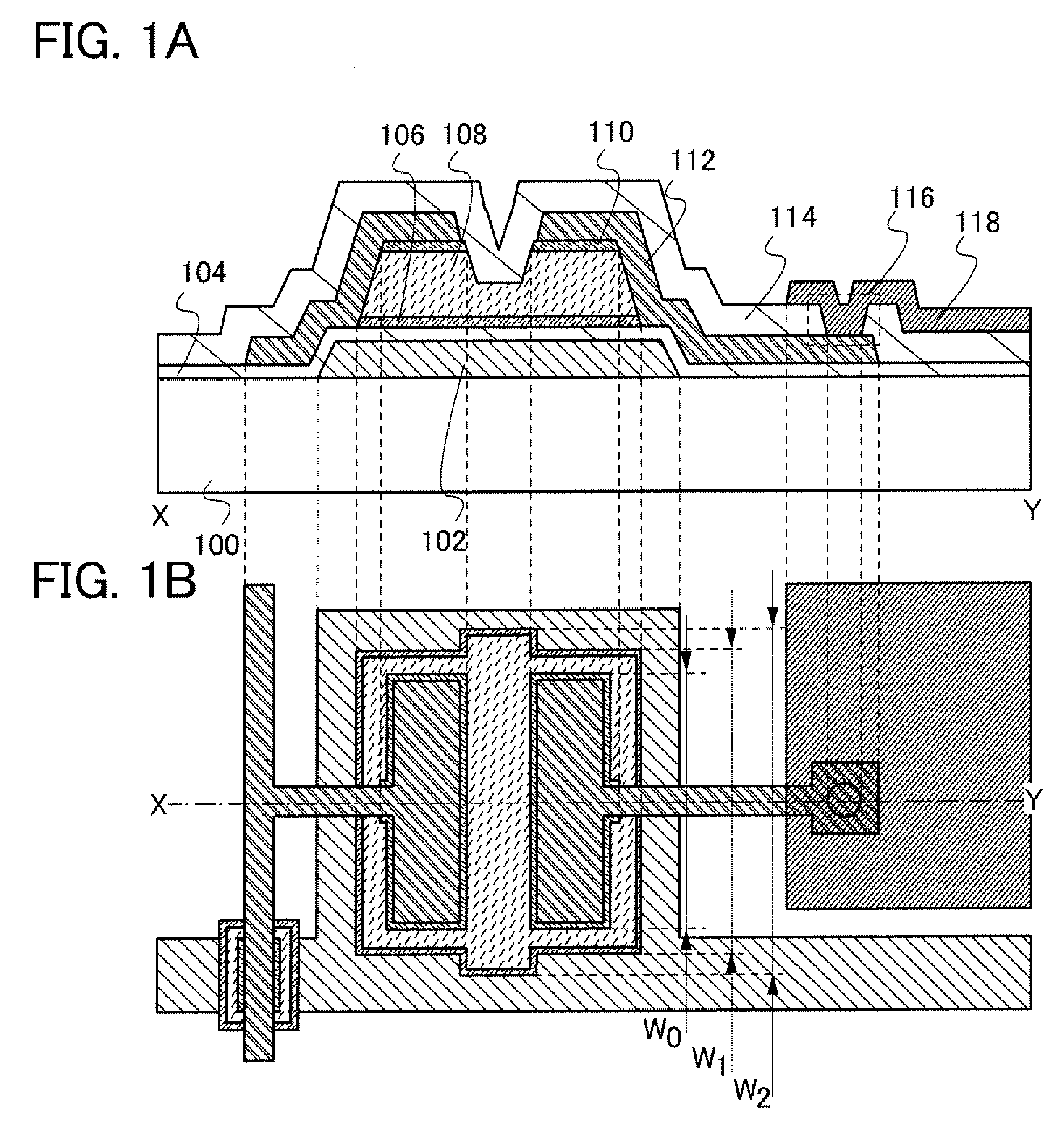
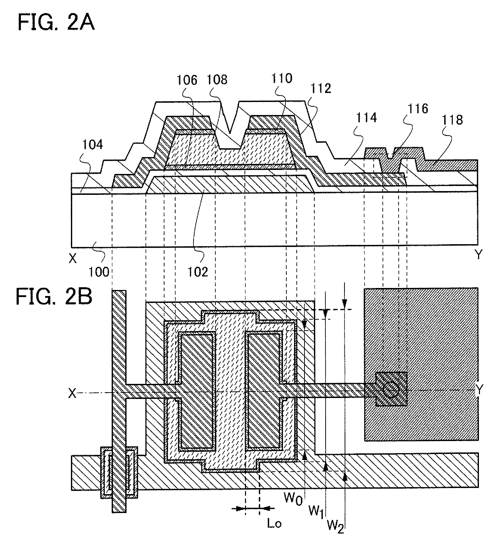
[0036]In this embodiment, a TFT according to one mode of the present invention will be described with reference to drawings.

[0037]According to one embodiment of the present invention, a thin film transistor includes a gate electrode; a gate insulating layer which is provided to cover the gate electrode; a semiconductor layer which is provided over the gate insulating layer to overlap with the gate electrode; an impurity semiconductor layer which is partly provided over the semiconductor layer and which forms a source region and a drain region; and a wiring layer which is provided over the impurity semiconductor layer, where a width of the source region and the drain region is narrower than a width of the semiconductor layer, and where the width of the semiconductor layer is increased at least in a portion between the source region and the drain region. Here, the gate electrode is formed using a first wiring layer, and source and drain electrodes are formed using a second wiring laye...

embodiment 2

[0142]In this embodiment, one mode of a display panel or a light-emitting panel on which the TFT described in Embodiment 1 is mounted will be described with reference to drawings.

[0143]In the display device or the light-emitting device according to this embodiment, a signal line driver circuit and a scan line driver circuit may be formed over a different substrate (e.g., a semiconductor substrate or an SOI substrate) and then connected to the pixel portion or may be formed over the same substrate as a pixel circuit.

[0144]Note that there are no particular limitations on the connection method of a substrate separately formed, and a known method such as a COG method, a wire bonding method, or a TAB method can be used. Further, a connection position is not limited as long as electrical connection is possible. Alternatively, a controller, a CPU, a memory, or the like may be formed separately and connected to the pixel circuit.

[0145]FIG. 16 illustrates a block diagram of a display device....

embodiment 3

[0167]In this embodiment, electronic devices in which a display panel or a display device manufactured by the method described in Embodiment 2 is incorporated as a display portion will be described with reference to FIGS. 19A and 19B, FIG. 20, and FIGS. 21A to 21C. As such electronic devices, for example, cameras such as video cameras or digital cameras; head mounted displays (goggle type displays); car navigation systems; projectors; car stereos; personal computers; and portable information terminals (such as mobile computers, mobile phones, and e-book readers) can be given. Examples of the electronic devices are illustrated in FIGS. 19A and 19B.

[0168]FIG. 19A illustrates a television device. A television device illustrated in FIG. 19A can be completed by incorporating a display panel into a housing. A main screen 503 is formed using the display panel manufactured by the manufacturing method described in Embodiment 2, and a speaker portion 509, operation switches, and the like are ...


PUM


Abstract

A thin film transistor includes a gate electrode; a gate insulating layer which is provided to cover the gate electrode; a semiconductor layer which is provided over the gate insulating layer to overlap with the gate electrode; an impurity semiconductor layer which is partly provided over the semiconductor layer and which forms a source region and a drain region; and a wiring layer which is provided over the impurity semiconductor layer, where a width of the source region and the drain region is narrower than a width of the semiconductor layer, and where the width of the semiconductor layer is increased at least in a portion between the source region and the drain region.

Description

BACKGROUND OF THE INVENTION[0001]1. Field of the Invention[0002]The present invention relates to a thin film transistor. In particular, the present invention relates to a display device provided with a thin film transistor.[0003]2. Description of the Related Art[0004]In recent years, a thin film transistor (hereinafter referred to as a TFT) including a semiconductor thin film (with a thickness of several nanometers to several hundreds of nanometers, approximately) over a substrate having an insulating surface (e.g., a glass substrate) have been attracting attention. TFTs are widely used for IC (integrated circuit) and electronic devices such as electro-optical devices. In particular, a TFT is rapidly developed as a switching element of image display devices typified by liquid crystal display devices and the like. In an image display device such as a liquid crystal display device, a TFT including an amorphous semiconductor film or a TFT including a polycrystalline semiconductor film ...

Claims


Application Information

Patent Timeline
IPC IPC(8): H01L33/16H01L29/786
CPCH01L21/67207H01L27/12H01L29/78696H01L29/78618H01L29/04H01L27/1214H01L29/458
Inventor MIYAIRI, HIDEKAZU
Owner SEMICON ENERGY LAB CO LTD
Why Eureka
Try Eureka