Element substrate and light emitting device

Inactive Publication Date: 2006-10-17
SEMICON ENERGY LAB CO LTD
View PDF6 Cites 30 Cited by
  • Summary
  • Abstract
  • Description
  • Claims
  • Application Information

AI Technical Summary

Benefits of technology

[0009]A transistor using a polycrystalline silicon film formed on a glass substrate by laser anneal and the like exhibits high field effect mobility and large amo

Problems solved by technology

However, characteristics of a transistor using a polycrystalline silicon vary easily due to a defect in a

Method used


Image

  • Element substrate and light emitting device
  • Element substrate and light emitting device
  • Element substrate and light emitting device

Examples


embodiment mode 1

[Embodiment Mode 1]

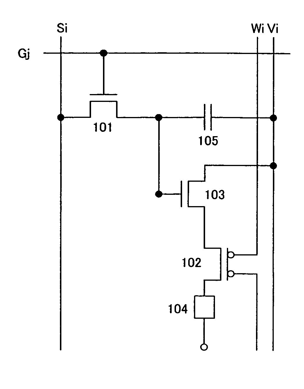
[0040]FIG. 1 shows an embodiment mode of a pixel of a light emitting device of the invention. The pixel shown in FIG. 1 comprises a light emitting element 104, a transistor (switching transistor) 101 used as a switching element for controlling an input of a video signal to the pixel, a driving transistor 102 for controlling an amount of current flowing in the light emitting element 104, and a current controlling transistor 103 for controlling a current supply to the light emitting element 104. In addition, a capacitor 105 for storing a video signal potential may be provided in the pixel.

[0041]Symbol for the driving transistor 102 in FIG. 1 is explained here. This symbol represents a transistor that two contact points are formed at the gate electrode, which is different from a typical connection. Therefore, the driving transistor 102 is specially represented by this symbol. That is, one end of the gate electrode and the other end thereof are connected to a wiring. ...

embodiment mode 2

[Embodiment Mode 2]

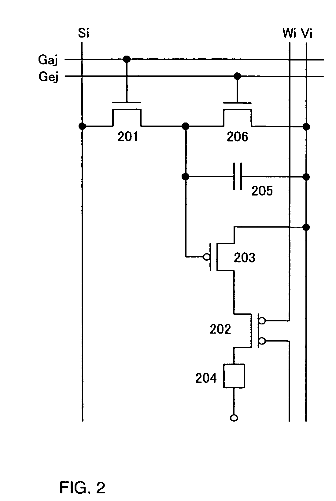
[0061]Described in this embodiment mode is a configuration of a pixel of the light emitting device of the invention, which is different from that shown in FIG. 1.

[0062]The pixel shown in FIG. 2 comprises a light emitting element 204, a switching transistor 201, a driving transistor 202, a current controlling transistor 203, and a transistor (erasing transistor) 206 for forcibly turning OFF the current controlling transistor 203. In addition, a capacitor 205 may be provided in the pixel.

[0063]The driving transistor 202 and the current controlling transistor 203 have the same conductivity. In the invention, the driving transistor 202 is operated in a saturation region and the current controlling transistor 203 is operated in a linear region.

[0064]A channel length L of the driving transistor 202 may be longer than its channel width W, and a channel length L of the current controlling transistor 203 may be equal to or shorter than its channel width W. Desirably, the r...

embodiment mode 3

[Embodiment Mode 3]

[0076]Described in this embodiment mode are a construction and the driving of a light emitting device having active matrix pixels driven by thin film transistors (TFTs).

[0077]FIG. 3 is a block diagram of an external circuit and a schematic diagram of a panel. An active matrix display device shown in FIG. 3 comprises an external circuit 3004 and a panel 3010. The external circuit 3004 comprises an A / D converter unit 3001, a power supply unit 3002, and a signal generator unit 3003. The A / D converter unit 3001 converts an image data signal which is input as an analog signal into a digital signal (video signal), and supplies it to a signal line driver circuit 3006. The power supply unit 3002 generates power having a predetermined voltage from power supplied by a battery or an outlet, and supplies the generated power to the signal line driver circuit 3006, scan line driver circuits 3007, a light emitting element 3011, the signal generator unit 3003, and the like. Power...


PUM


Abstract

No need of lowering off-current of a switching transistor, fewer luminance variations of a light emitting element between pixels due to characteristic variations of a driving transistor, and less risk of steps due to increase in the number of wirings. A video signal for light emission or non-emission of a pixel is input to a gate of a current controlling transistor operated in a linear region, which is connected in series with the driving transistor, through a switching transistor. Since a voltage Vds between a source and a drain of the current controlling transistor is small, small changes in a voltage Vgs between a gate and a source thereof do not affect a current flowing in a load. The current flowing in the light emitting element is determined by the driving transistor operated in a saturation region, and a fixed potential is input to the gate thereof during light emission.

Description

BACKGROUND OF THE INVENTION[0001]1. Field of the Invention[0002]The present invention relates to a light emitting device with a control system for light emission of a light emitting element and to an element substrate including the control system.[0003]2. Description of the Related Art[0004]In display panels using an organic electroluminescence medium, a flat panel formed of pixels using thin film transistors has been disclosed (e.g., see Patent Document 1). A configuration and an operation of a pixel included in such a conventionally well known flat panel are described in brief hereinafter with reference to drawings.[0005]A pixel shown in FIG. 7 comprises a switching transistor 700 whose gate is connected to a scan line 705, either a source or a drain of which is connected to a signal line 704 and the other is connected to a gate of a driving transistor 701. A source of the driving transistor 701 is connected to a power supply line 706 and a drain thereof is connected to an anode o...

Claims


Application Information

Patent Timeline
IPC IPC(8): G09G3/10G09G3/00G09G3/20G09G3/30G09G3/32G09G5/00H01L27/12H01L27/15H01L27/32H01L51/30H05B33/00
CPCG09G3/3233G09G3/3275G09G5/006G09G3/2022G09G2300/04G09G2300/0426G09G2300/0439G09G2300/0465G09G2300/08G09G2300/0842G09G2300/0861G09G2310/061G09G2320/043H01L27/12H01L27/3244H01L27/3276H10K59/12H10K59/131
Inventor FUKUMOTO, RYOTAANAZAI, AYAYAMAZAKI, YUOSAME, MITSUAKI
Owner SEMICON ENERGY LAB CO LTD
Why Eureka
Try Eureka