Element substrate and light emitting device

a technology of light emitting device and element substrate, which is applied in the direction of static indicating device, lighting and heating apparatus, instruments, etc., can solve the problems of variable characteristics and other problems, and achieve the effect of increasing the storage capacity of capacitors, reducing the cause of variation, and enhancing image quality

Active Publication Date: 2008-04-15
SEMICON ENERGY LAB CO LTD
View PDF9 Cites 33 Cited by
  • Summary
  • Abstract
  • Description
  • Claims
  • Application Information

AI Technical Summary

Benefits of technology

[0017]Since the current controlling transistor operates in a linear region, its source-drain voltage Vds is small, and small changes in a gate-source voltage Vgs of the current controlling transistor do not influence the current supplied to a light emitting element. Current supplied to the light emitting element is determined by the driving transistor which operates in a saturation region. A gate potential of the driving transistor corresponds to a potential of the second scan line, and a source potential of the driving transistor corresponds to a drain potential of the current controlling transistor. The gate-source voltage Vgs of the driving transistor is steady while the light emitting element emits lig

Problems solved by technology

However, the transistor using polysilicon has problems in that it is likely to

Method used


Image

  • Element substrate and light emitting device
  • Element substrate and light emitting device
  • Element substrate and light emitting device

Examples


embodiment mode 1

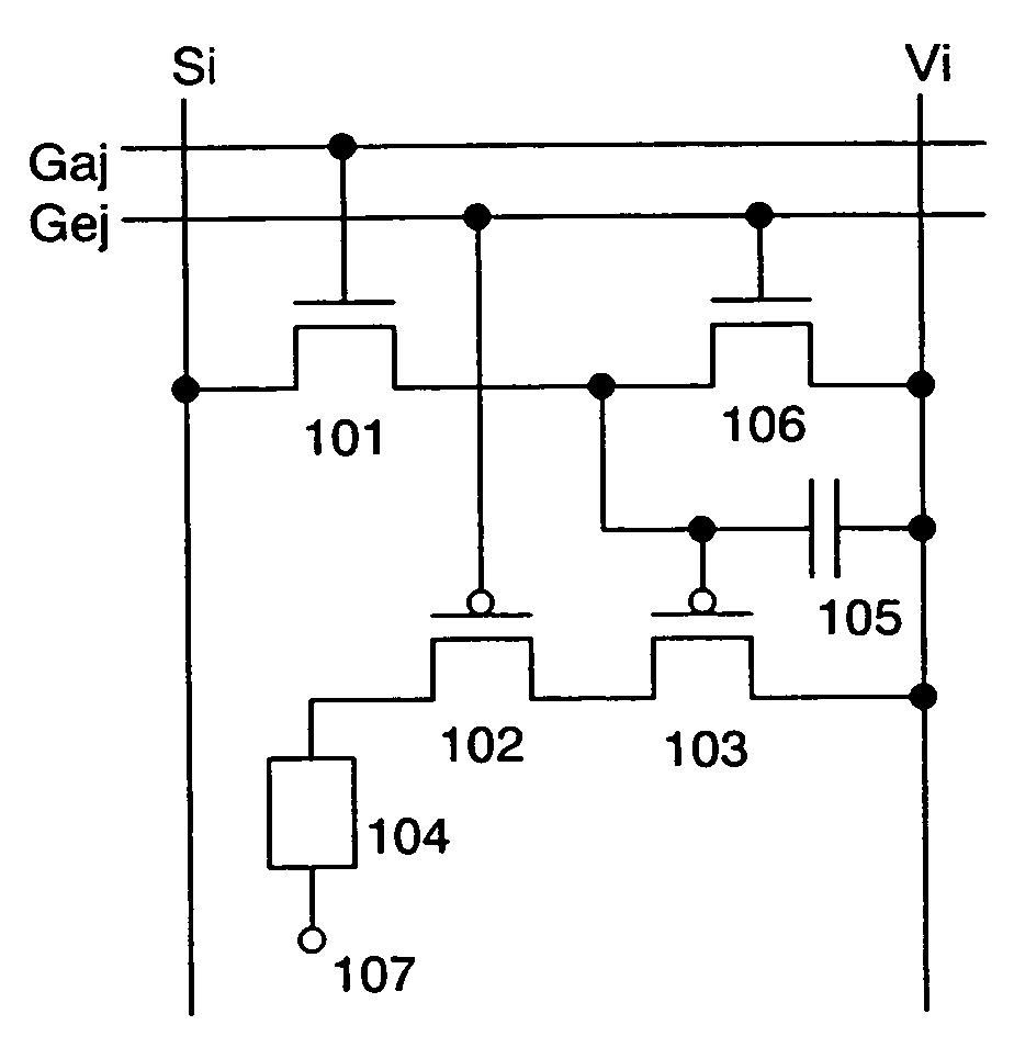
[0040]FIG. 1 shows an embodiment mode of a pixel of the light emitting device of the invention. The pixel shown in FIG. 1 comprises a light emitting element 104, a transistor (switching transistor) 101 used as a switching element for controlling a video signal input to the pixel, a driving transistor 102 for controlling a current value flowing in the light emitting element 104, a current controlling transistor 103 for controlling a current supply (or controlling a light emission or non-emission) to the light emitting element 104, and a transistor (erasing transistor) 106 for turning OFF the current controlling transistor 103 forcibly. In addition, it is also possible to dispose a capacitor 105 for storing a potential of a video signal as shown in this embodiment mode.

[0041]The driving transistor 102 and the current controlling transistor 103 have the same polarity, while the erasing transistor 106 and the driving transistor 102 have the opposite polarity to each other. In addition, ...

embodiment mode 2

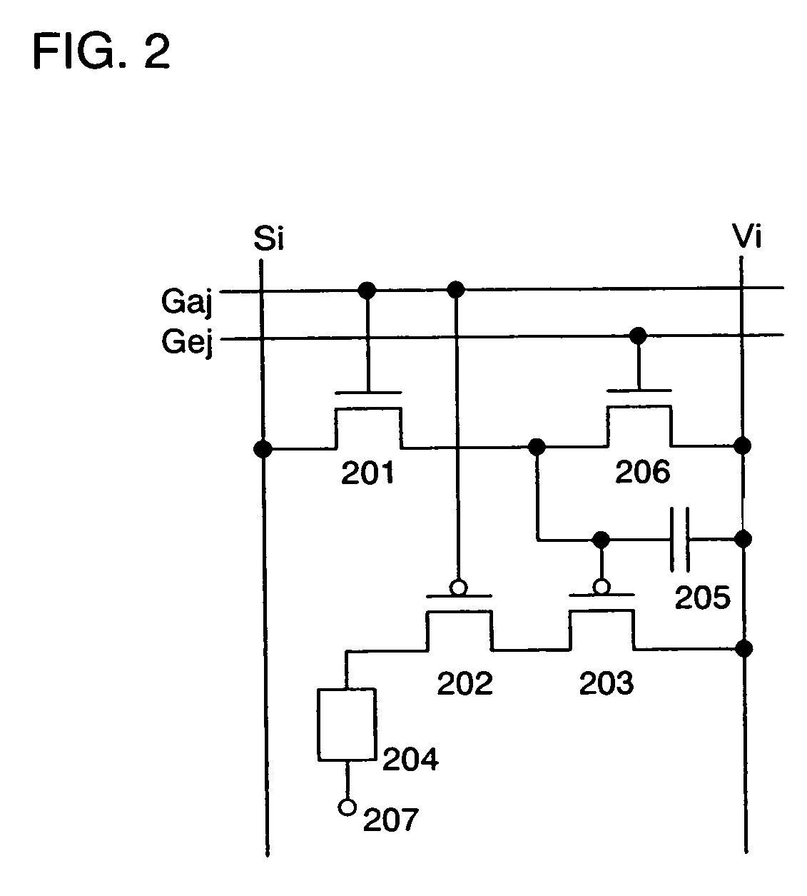
[0070]Described in this embodiment mode is another pixel configuration of the light emitting device of the invention which is different from that shown in FIG. 1.

[0071]The pixel shown in FIG. 2 comprises a light emitting element 204, a switching transistor 201, a driving transistor 202, a current controlling transistor 203, and an erasing transistor 206. It is also possible to dispose a capacitor 205 in addition to these elements.

[0072]The driving transistor 202 and the current controlling transistor 203 have the same polarity, while the switching transistor 201 and the driving transistor 202 have the opposite polarity to each other. According to the invention, the driving transistor 202 operates in a saturation region while the current controlling transistor 203 operates in a linear region.

[0073]The channel length (L) of the driving transistor 202 may be longer than its channel width (W), and L of the current controlling transistor 203 may be equal to or shorter than its W. Desirab...

embodiment 1

[0092]Described in this embodiment are a configuration of an active matrix display device to which the pixel configuration of the invention is applied and its drive.

[0093]FIG. 8 shows a block diagram of an external circuit and a schematic view of a panel.

[0094]An active matrix display device shown in FIG. 8 comprises an external circuit 8004 and a panel 8010. The external circuit 8004 comprises an A / D converter unit 8001, a power supply unit 8002, and a signal generator unit 8003. The A / D converter unit 8001 converts an image data signal which is input as an analog signal into a digital signal (video signal), and supplies it to a signal driver circuit 8006. The power supply unit 8002 generates power having a desired level of voltage from the power supplied from a battery or an outlet, and supplies it to the signal driver circuit 8006, a first scan driver circuit 8007 a second scan driver circuit 8012, a light emitting element 8011, the signal generator unit 8003, and the like. The s...


PUM


Abstract

A light emitting device and an element substrate which are capable of suppressing variations in luminance intensity of a light emitting element among pixels due to characteristic variations of a driving transistor without suppressing off-current of a switching transistor low and increasing storage capacity of a capacitor. A gate potential of a driving transistor is connected to a first scan line or a second scan line, and the driving transistor operates in a saturation region. A current controlling transistor which operates in a linear region is connected in series to the driving transistor. A video signal which transmits a light emission or non-emission of a pixel is input to the gate of the current controlling transistor through a switching transistor.

Description

BACKGROUND OF THE INVENTION[0001]1. Field of the Invention[0002]The present invention relates to a light emitting device comprising a plurality of pixels each including a light emitting element and a means for supplying current to the light emitting element.[0003]2. Description of the Related Art[0004]Since a light emitting element emits light by itself, it is highly visible and does not require a back light which is needed in a liquid crystal display device (LCD). Therefore, it is suitably applied to thin devices and not restricted in viewing angle. Because of these advantages, a light emitting device having a light emitting element has recently been drawing attentions as an alternative display device to a CRT and an LCD. It is to be noted that a light emitting element in this specification indicates an element whose luminance is controlled by current or voltage, and it includes an OLED (Organic Light Emitting Diode) or an MIM electron source element (electron discharge element) an...

Claims


Application Information

Patent Timeline
IPC IPC(8): G09G3/32H01L51/50G09G3/20G09G3/22G09G3/30H01L27/32H01L51/52H03K3/42H05B33/14
CPCG09G3/3233G09G3/2022G09G3/3266G09G3/3291G09G2300/0426G09G2300/0814G09G2300/0842G09G2300/0861G09G2310/0251G09G2320/0233H01L27/322H01L27/3244H01L27/3295H01L51/5221H01L2251/5323H10K59/38H10K59/1216H10K59/1213H10K59/122H10K59/131H10K50/828H10K2102/3031H10K50/82H10K59/12F21V23/001F21V23/06G09G2310/0286G09G2310/0289G09G2310/0291G09G2330/021H01L27/1222H01L27/124H01L27/1251H01L29/78696
Inventor YAMAZAKI, YUANZAI, AYAOSAME, MITSUAKI
Owner SEMICON ENERGY LAB CO LTD
Why Eureka
Try Eureka