Trench gate charge storage reverse-conducting insulated-gate bipolar transistor (RC-IGBT) and fabrication method thereof
A technology of charge storage and charge storage layer, which is applied in semiconductor/solid-state device manufacturing, circuits, electrical components, etc., and can solve the compromise characteristics of the conduction voltage drop and switching loss that affect the device, the large forward conduction voltage drop, and the reduction of the device switching speed etc.
- Summary
- Abstract
- Description
- Claims
- Application Information
AI Technical Summary
Problems solved by technology
Method used
Image
Examples
Embodiment 1
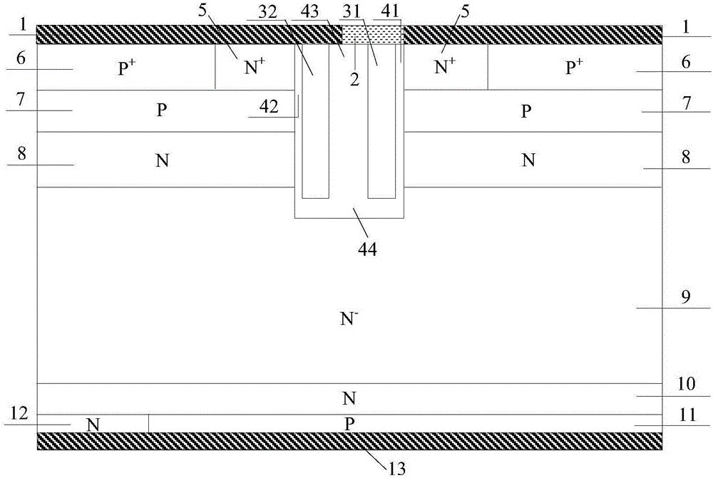
[0043] In this example, a trench gate charge storage type RC-IGBT, its cell structure is as follows figure 2As shown, it includes: the back collector metal 13, the P-type collector region 11 and the N-type collector region 12 located on the back collector metal 13 and connected to it, and the P-type collector region 11 and the N-type collector region The N-type field stop layer 10 above and connected to the N-type field stop layer 10, the N-drift region 9 located on the N-type field stop layer 10 and connected to it; the composite trench structure located in the middle of the upper part of the N-drift region 9 and connected to it; The N-type charge storage layer 8 located on both sides of the upper part of the N-drift region 9 and connected to it, the side wall of the N-type charge storage layer 8 is connected to the side wall of the composite trench structure, located on the upper part of the N-type charge storage layer 8 and The p-type base region 7 connected to it, the sid...
Embodiment 2
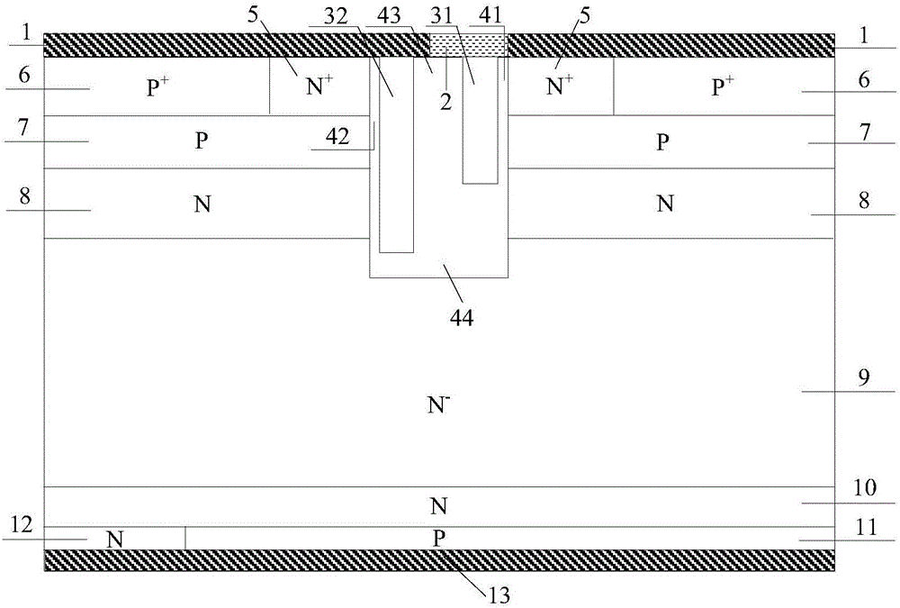
[0045] In this example, a trench gate charge storage type RC-IGBT, its cell structure is as follows image 3 As shown, it includes: the back collector metal 13, the P-type collector region 11 and the N-type collector region 12 located on the back collector metal 13 and connected to it, and the P-type collector region 11 and the N-type collector region The N-type field stop layer 10 above and connected to the N-type field stop layer 10, the N-drift region 9 located on the N-type field stop layer 10 and connected to it; the composite trench structure located in the middle of the upper part of the N-drift region 9 and connected to it; The N-type charge storage layer 8 located on both sides of the upper part of the N-drift region 9 and connected to it, the side wall of the N-type charge storage layer 8 is connected to the side wall of the composite trench structure, located on the upper part of the N-type charge storage layer 8 and The p-type base region 7 connected to it, the sid...
PUM
| Property | Measurement | Unit |
|---|---|---|
| Thickness | aaaaa | aaaaa |
| Thickness | aaaaa | aaaaa |
| Thickness | aaaaa | aaaaa |
Abstract
Description
Claims
Application Information


