Transistor having recess channel and fabricating method thereof

a technology of metal oxide semiconductor and recess channel, which is applied in the direction of semiconductor devices, basic electric elements, electrical appliances, etc., can solve the problems of limitation in improving the switching speed of the dmos device functioning as a switching device, and the normal operation has become difficult to perform, so as to reduce the gate capacitance and improve the switching speed of the device

Active Publication Date: 2010-08-03
KEY FOUNDRY CO LTD
View PDF13 Cites 11 Cited by
  • Summary
  • Abstract
  • Description
  • Claims
  • Application Information

AI Technical Summary

Benefits of technology

[0008]Embodiments of the present invention are directed to provide a recess transistor and a method for fabricating the same, which can improve a switching speed of a device by reducing a gate capacitance.

Problems solved by technology

As a result, in the MOSFET device having a horizontal channel, which is a typical structure, normal operations have become difficult to perform because of a short channel effect (SCE) and a drain induced barrier lower (DIBL) effect derived from the reduced channel length between a source and a drain.
Accordingly, there are limitations in improving a switching speed of the DMOS device functioning as a switching device.

Method used


Image

  • Transistor having recess channel and fabricating method thereof
  • Transistor having recess channel and fabricating method thereof
  • Transistor having recess channel and fabricating method thereof

Examples


Embodiment Construction

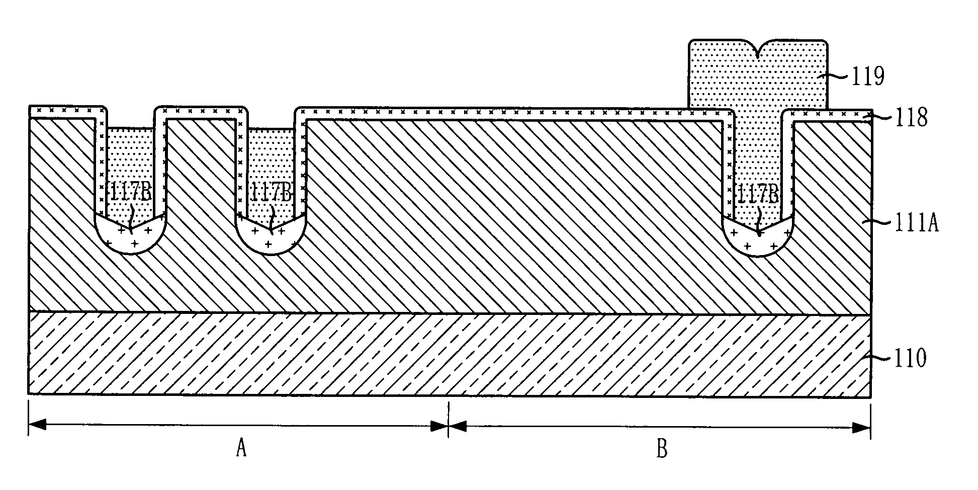
[0017]A transistor having a recess channel and a fabricating method thereof in accordance with various embodiments of the present invention will be described in detail with reference to the accompanying drawings. Also, regarding the drawings, the illustrated thickness of layers and regions are exaggerated for definitude. When a first layer is referred to as being on a second layer or “on” a substrate, it could mean that the first layer is formed right on the second layer or the substrate, or it could also mean that a third layer may exit between the first layer and the substrate. Furthermore, the same or like reference numerals through out the various embodiments of the present invention represent the same or like elements in different drawings.

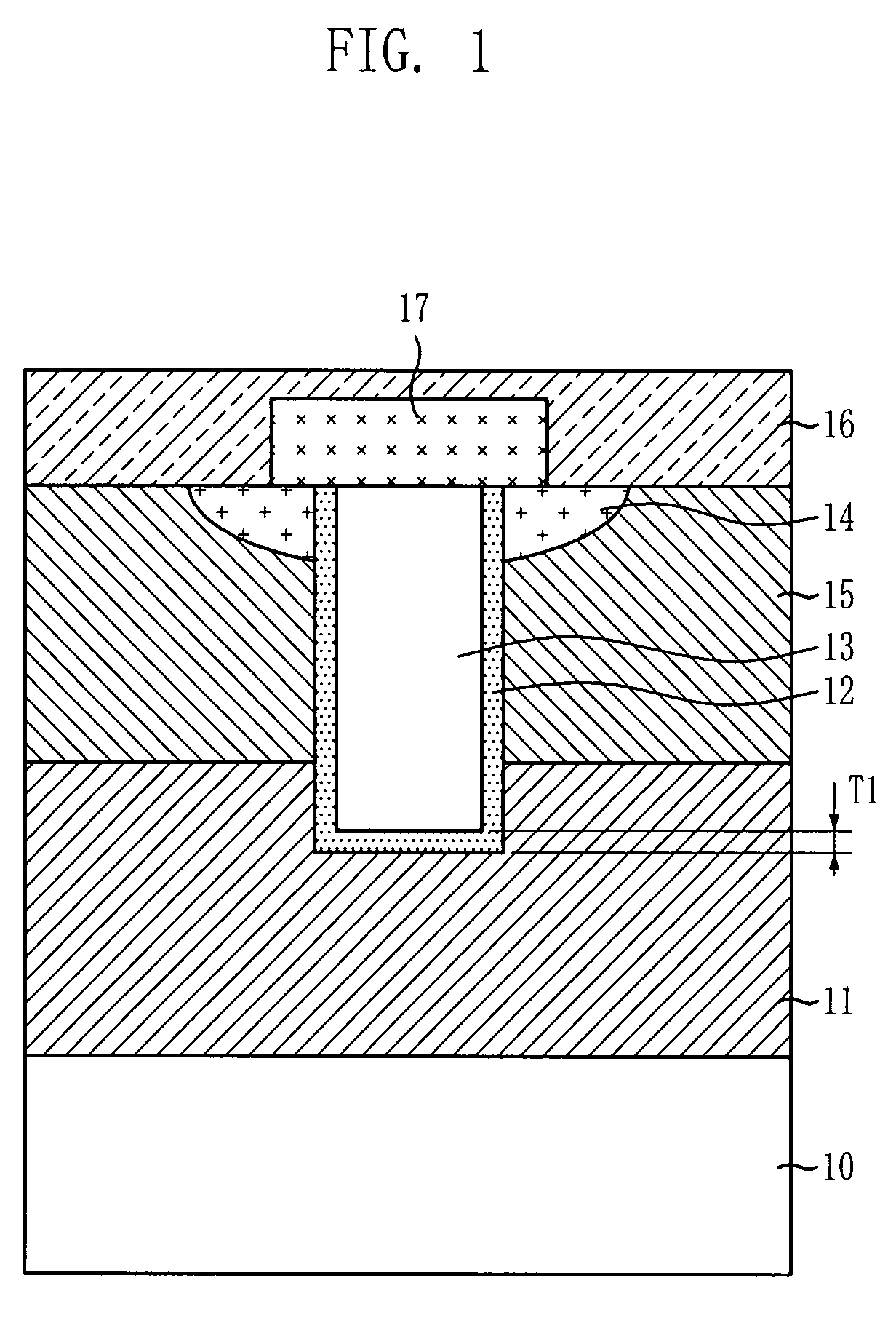
[0018]FIG. 2 illustrates a cross-sectional view of a double diffused metal-oxide semiconductor (DMOS) device in accordance with an embodiment of the present invention. In this embodiment, a thickness of a gate oxide layer 22 formed at the bot...


PUM


Abstract

A transistor includes a substrate including a trench, an insulation layer filled in a portion of the trench, the insulation layer having a greater thickness over an edge portion of a bottom surface of the trench than over a middle portion of the bottom surface of the trench, a gate insulation layer formed over inner sidewalls of the trench, the gate insulation layer having a thickness smaller than the insulation layer, and a gate electrode filled in the trench.

Description

CROSS-REFERENCE TO RELATED APPLICATIONS[0001]The present invention claims priority of Korean patent application number 10-2006-0133855, filed on Dec. 26, 2006, which is incorporated by reference in its entirety.BACKGROUND OF THE INVENTION[0002]The present invention relates to a method for fabricating a semiconductor device, and more particularly, to a method for fabricating a metal-oxide semiconductor field effect transistor (MOSFET) having a recess channel.[0003]A typical semiconductor device has adopted an individual device, such as a MOSFET device, as a switching device. Accordingly, the size of the MOSFET device has decreased as the semiconductor device becomes highly integrated. As a result, in the MOSFET device having a horizontal channel, which is a typical structure, normal operations have become difficult to perform because of a short channel effect (SCE) and a drain induced barrier lower (DIBL) effect derived from the reduced channel length between a source and a drain.[00...

Claims


Application Information

Patent Timeline
Patent Type & Authority Patents(United States)
IPC IPC(8): H01L29/94
CPCH01L29/7813H01L29/66734H01L29/42368H01L29/7811H01L21/18
Inventor CHO, CHEOL-HO
Owner KEY FOUNDRY CO LTD
Why Eureka
Try Eureka