Thin film transistor and active matrix organic light emitting diode component and manufacturing method

A thin-film transistor and source technology, applied in semiconductor/solid-state device manufacturing, transistors, electrical solid-state devices, etc., can solve the problems of product electrical property difference, silicon oxide loss, dopant injection distribution difference, etc., and achieve good TFT performance Consistency, gate insulation loss reduction, effect of reducing GIDL

Active Publication Date: 2017-09-01
EVERDISPLAY OPTRONICS (SHANGHAI) CO LTD
View PDF7 Cites 0 Cited by
  • Summary
  • Abstract
  • Description
  • Claims
  • Application Information

AI Technical Summary

Problems solved by technology

At this time, the underlying insulating layer such as the silicon oxide layer 116' may also be etched, resulting in loss of silicon oxide (such as figure 1 circled part in)
As a result, the dopant implantation profile of the source region S and the drain region D will therefore be different, and thus lead to differences in the electrical properties (such as Ion, Ioff, Vth, mobility, etc.) of the final product

Method used


Image

  • Thin film transistor and active matrix organic light emitting diode component and manufacturing method
  • Thin film transistor and active matrix organic light emitting diode component and manufacturing method
  • Thin film transistor and active matrix organic light emitting diode component and manufacturing method

Examples


Embodiment Construction

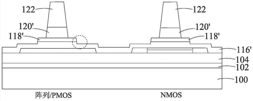
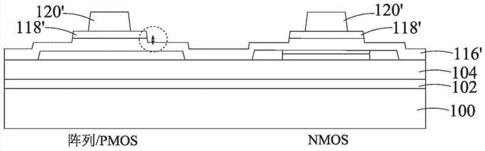
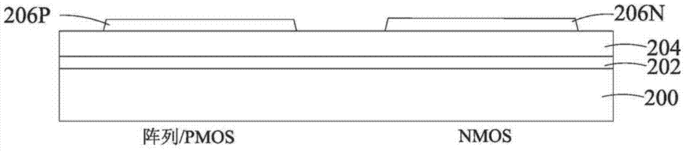
[0032] Example embodiments will now be described more fully with reference to the accompanying drawings. Example embodiments may, however, be embodied in many forms and should not be construed as limited to the embodiments set forth herein; rather, these embodiments are provided so that this disclosure will be thorough and complete, and will fully convey the concept of example embodiments to those skilled in the art. In the drawings, the thickness of regions and layers are exaggerated for clarity. The same reference numerals in the drawings denote the same or similar structures, and thus their detailed descriptions will be omitted.

[0033] Furthermore, the described features, structures, or characteristics may be combined in any suitable manner in one or more embodiments. In the following description, numerous specific details are provided in order to give a thorough understanding of embodiments of the present disclosure. However, one skilled in the art will appreciate tha...


PUM


Abstract

The application provides a thin film transistor, an active matrix organic light emitting diode assembly and a manufacturing method. A thin film transistor comprising: a substrate; a buffer layer on the substrate; a semiconductor layer on the buffer layer, including a source region, a drain region and a channel region; a first gate insulating layer covering the semiconductor layer; The foot of the second gate insulation layer located on the first gate insulation layer, the width of the foot of the second gate insulation layer is smaller than the width of the first gate insulation layer; the foot of the second gate insulation layer A gate electrode on the upper surface, wherein the portion of the first gate insulating layer on the semiconductor layer has a flat upper surface.

Description

technical field [0001] The present disclosure relates to an active matrix organic light emitting display, and in particular, to a thin film transistor, an active matrix organic light emitting diode (AMOLED) assembly including the thin film transistor, and a method of manufacturing the thin film transistor. Background technique [0002] The thin film transistor (TFT) array component part of an active matrix organic light emitting diode (Active Matrix Organic Light Emitting Diode: AMOLED) generally adopts a low temperature polysilicon (LTPS: Low Temperature Poly Silicon) process. The quality of thin film transistors and array components including thin film transistors will also determine the final display quality of AMOLED. [0003] In the process of manufacturing AMOLED_LTPS TFT, see Figure 1-2 , using the photoresist pattern 122 as a mask, etch a part of the gate metal layer and the gate insulating layer to form a gate line (not shown), a gate electrode 120 ′ and, for examp...

Claims


Application Information

Patent Timeline
Patent Type & Authority Patents(China)
IPC IPC(8): H01L29/423H01L29/49H01L21/336H01L29/786H01L27/12H01L21/77
CPCH10K59/122H10K59/12H10K50/805H01L29/42384H01L29/4908H01L29/66757H01L29/78621H01L2029/42388H01L27/127H10K59/1213
Inventor 许嘉哲黄家琦陈韦廷许民庆
Owner EVERDISPLAY OPTRONICS (SHANGHAI) CO LTD
Why Eureka
Try Eureka