Electronic device including a high electron mobility transistor including a gate electrode and a dielectric film

a high electron mobility, transistor technology, applied in the direction of semiconductor devices, basic electric elements, electrical equipment, etc., can solve the problems of reducing device reliability, affecting device reliability, and affecting the reliability of devices

Active Publication Date: 2020-10-27
SEMICON COMPONENTS IND LLC
View PDF17 Cites 1 Cited by
  • Summary
  • Abstract
  • Description
  • Claims
  • Application Information

AI Technical Summary

Benefits of technology

[0027]Features of a high electron mobility transistor (HEMT) can be used and improve performance of the HEMT. An extension region of a lower dielectric film can locally increase a sheet resistance of a two dimensional electron gas (2DEG) near a gate electrode and allow for faster depletion of charge. The locally higher sheet resistance can be designed so RDSON for the HEMT may not increase by more than 1 ohm·mm. An upper dielectric film can help reduce sheet resistance of the 2DEG to help counter some of the increased sheet resistance corresponding to the lower dielectric film. Cm can be lower and provide a lower Miller ratio. Output capacitance (COSS) for the HEMT is lower. Thus, the HEMT has improved switching characteristics. The lower dielectric film can cover corners of portions of a top surface of the gate electrode and help with more uniform subthreshold slope during turn on and increase the gate breakdown voltage.

Problems solved by technology

Improving one variable typically comes at the expense of one of the other parameters.
For example, improving resistance to gate bounce may be accompanied by lower device reliability, increased uniformity in subthreshold slope may be accompanied by higher RDSON, etc.

Method used


Image

  • Electronic device including a high electron mobility transistor including a gate electrode and a dielectric film
  • Electronic device including a high electron mobility transistor including a gate electrode and a dielectric film
  • Electronic device including a high electron mobility transistor including a gate electrode and a dielectric film

Examples


embodiment 1

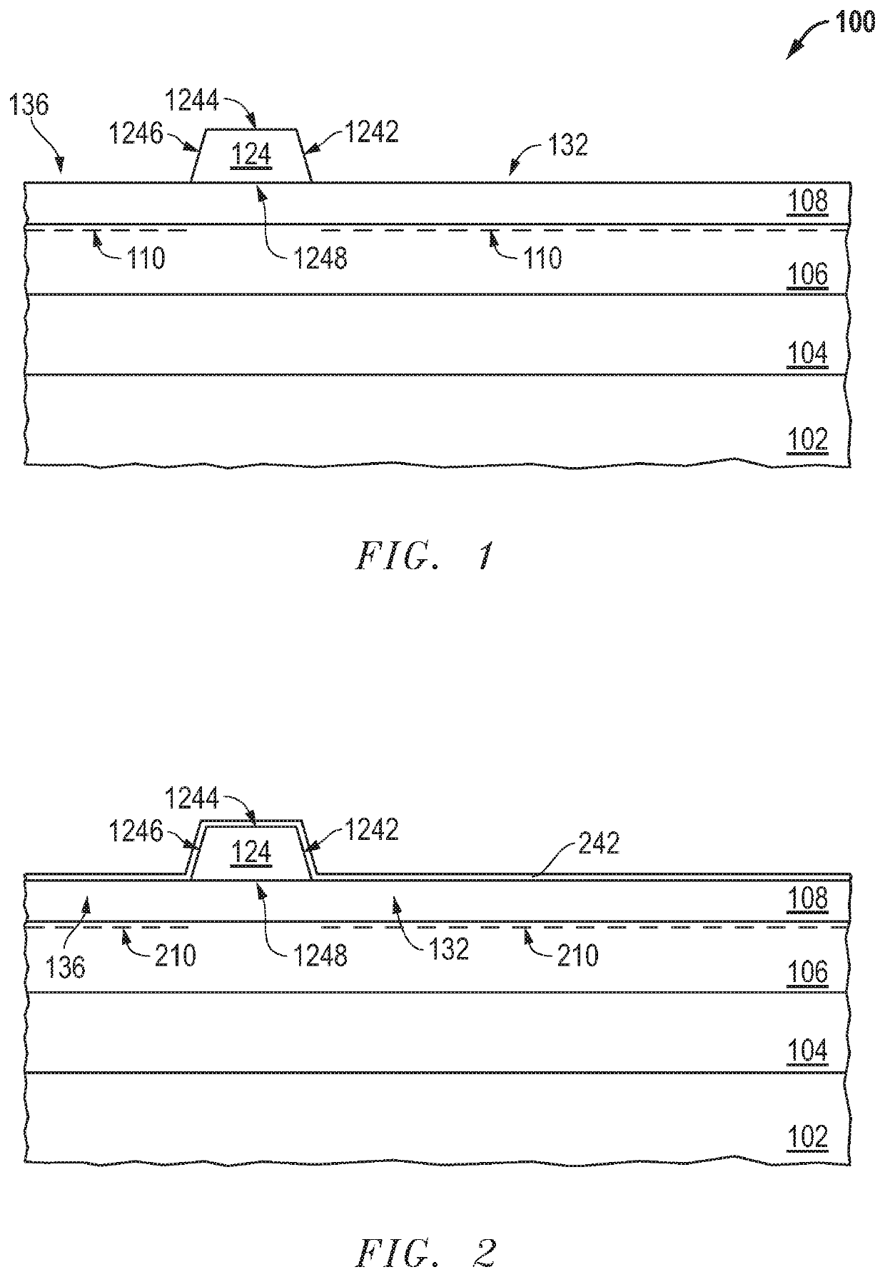
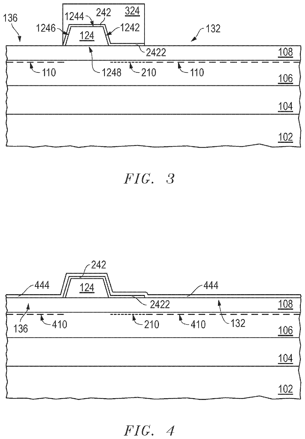
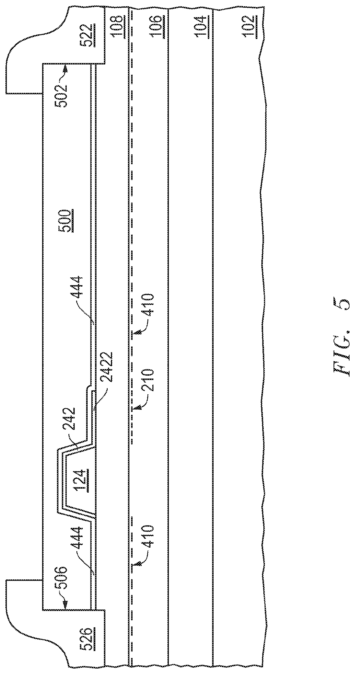
[0074]An electronic device including a high electron mobility transistor including a gate electrode; a drain electrode; an access region including a first portion closer to the gate electrode and a second portion closer to the drain electrode; a first dielectric film including a first material and overlying the first portion and not the second portion of the access region; and a second dielectric film including a second material and overlying the second portion of the access region, wherein the second material is different from the first material.

embodiment 2

[0075]The electronic device of Embodiment 1, wherein the first dielectric film includes Si3N4, SiOkN1, where krNs, where r2O3, AlOtNu, where t>u, SiO2, HfO2, SiOmNn, where m>n, or another oxygen-containing dielectric material that provides a positively charged dielectric film.

embodiment 3

[0076]The electronic device of Embodiment 1, wherein the gate electrode has a top surface and a first sidewall that meet at a first corner, and the first dielectric film contacts the top surface and sidewall of the gate electrode at the first corner.


PUM

PropertyMeasurementUnit
thicknessaaaaaaaaaa
thicknessaaaaaaaaaa
thicknessaaaaaaaaaa

Abstract

An electronic device can include a HEMT. In an embodiment, a gate electrode, a drain electrode, and an access region including a first portion closer to the gate electrode and a second portion closer to the drain electrode. A lower dielectric film can overlie a portion of the access region, and an upper dielectric region can overlie another portion of the access region. In another embodiment, a dielectric film can have a relatively positive or negative charge and a varying thickness. In a further embodiment, the HEMT can include a gate electrode; a dielectric film overlying the gate electrode and defining openings to the gate electrode, wherein a portion of the dielectric film is disposed between the openings; and a gate interconnect extending into the openings of the dielectric film and contacting the gate electrode and the portion of the dielectric film.

Description

CROSS REFERENCE TO RELATED APPLICATION[0001]This application claims priority under 35 U.S.C. § 119(e) to U.S. Patent Application No. 62 / 835,592 entitled “Electronic Device Including a High Electron Mobility Transistor Including a Gate Electrode and a Dielectric Film,” by Banerjee et al., filed Apr. 18, 2019, which is assigned to the current assignee hereof and incorporated herein by reference in its entirety.FIELD OF THE DISCLOSURE[0002]The present disclosure relates to electronic devices, and more particularly to, electronic devices including high electron mobility transistors including gate electrodes and dielectric films.RELATED ART[0003]Enhancement-mode high electron mobility transistors can have a gate field electrode extending toward the drain electrode to help with device reliability. However, the gate field electrode can increase the gate-to-drain capacitance, CGD, that results in a higher Miller ratio, which is CGD / CGS, where CGS is the gate-to-source capacitance. Other par...

Claims


Application Information

Patent Timeline
Patent Type & Authority Patents(United States)
IPC IPC(8): H01L29/778H01L29/423H01L29/417H01L29/40H01L29/20H01L29/51
CPCH01L29/41725H01L29/512H01L29/2003H01L29/402H01L29/7786H01L29/42316H01L29/1066H01L29/408H01L29/41766H01L29/66462
Inventor BANERJEE, ABHISHEKMOENS, PETER
Owner SEMICON COMPONENTS IND LLC
Why Eureka
Try Eureka