Metal oxide semiconductor (mos) transistors with increased break down voltages and methods of making the same

A transistor and gate oxide technology, applied in semiconductor devices, circuits, electrical components, etc., can solve problems such as increasing the cost of MOS transistors, and achieve the effect of increasing gate breakdown voltage

Active Publication Date: 2011-06-29
AOTU ELECTRONICS WUHAN
View PDF0 Cites 1 Cited by
  • Summary
  • Abstract
  • Description
  • Claims
  • Application Information

AI Technical Summary

Problems solved by technology

However, the above methods require additional processing steps and additional masks which increase the cost of the MOS transistors

Method used


Image

  • Metal oxide semiconductor (mos) transistors with increased break down voltages and methods of making the same
  • Metal oxide semiconductor (mos) transistors with increased break down voltages and methods of making the same
  • Metal oxide semiconductor (mos) transistors with increased break down voltages and methods of making the same

Examples


Embodiment Construction

[0017] Specific embodiments of the present invention will be described below. The invention will be described in connection with some specific embodiments of the invention, but the invention is not limited to the specific embodiments described. Any modifications or equivalent replacements made to the present invention shall fall within the scope of the claims of the present invention.

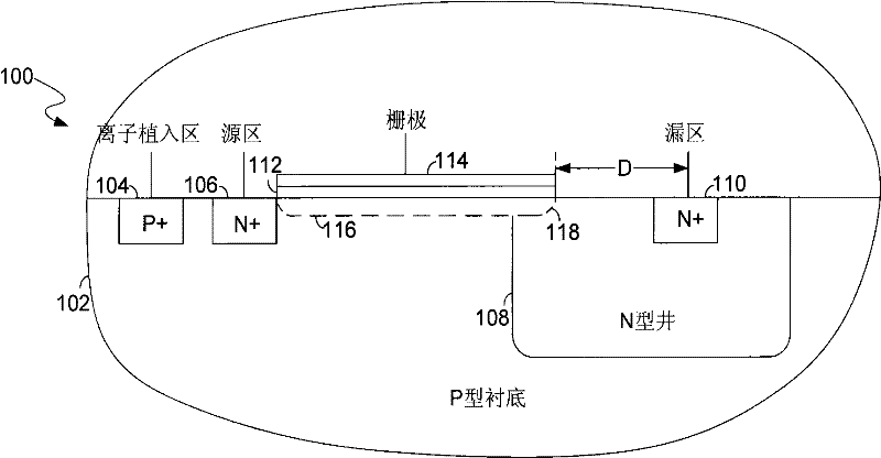
[0018] In one embodiment, the present invention provides a MOS transistor with an improved gate breakdown voltage that can operate at relatively high voltages. In this embodiment, the MOS transistors may be arranged in a predetermined shape (eg, circular) that counteracts junction curvature effects. Therefore, without additional processing steps and masks, the gate breakdown voltage of the MOS transistor can be increased.

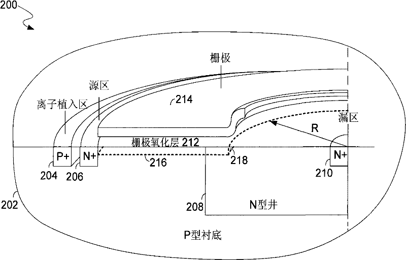
[0019] figure 2 Shown is a perspective view of the left half of MOS transistor 200 in accordance with an embodiment of the present invention. MOS transistor 200 may be ...


PUM


Abstract

The present invention discloses a transistor that breakdown voltage improvement and making method thereof, wherein the transistor comprises the following components: a substrate in a first conductive type and a first adulterate concentration; a drain region and a source region disposed in the substrate and have a second conductive type; a grid disposed in the source region and the drain region, wherein the grid and the substrate is separated by a grid oxidizing layer; a adjust implant region disposed on the substrate below the grid oxidizing layer and has the first conductive type, wherein the adjust implant region is provided with a second adulterate concentration higher than the first adulterate concentration; and planar junction formed between the adjust implant region and the drain region, wherein the adjust implant region and the drain region is provided with a preset shape for the sake of forming the planar junction with surface curvature pointing at the drain region, and release electric field intensity where the planar junction locates for further.

Description

technical field [0001] The invention relates to semiconductor components, especially high-voltage MOS transistors. Background technique [0002] Many applications of semiconductor devices require MOS transistors that can operate at relatively high voltages. figure 1 A cross-sectional view of a high voltage MOS transistor (eg, NMOS transistor 100 ) is shown. NMOS transistor 100 may be fabricated in P-type substrate 102 . In the P-type substrate 102, a P+ type ion implantation region 104 (body region) with a high doping concentration, an N+ type source region 106 (source electrode) with a high doping concentration and a drain with a low doping concentration can be formed. The region is implanted in an N-well 108 (N-well). An N+ type drain region 110 (drain) with high doping concentration can be formed in the N type well 108 . A gate oxide layer 112 may be formed above the P-type substrate region between the source 106 and the drain 110 . A gate 114 may be formed on the ga...

Claims


Application Information

Patent Timeline
Patent Type & Authority Patents(China)
IPC IPC(8): H01L29/78
CPCH01L29/0688H01L29/42368H01L29/4238H01L29/105H01L29/7835H01L29/66659H01L29/0692
Inventor 玛利安·乌德瑞·斯班内肖邦-米哈依·庞贝斯库拉兹洛·利普赛依
Owner AOTU ELECTRONICS WUHAN
Why Eureka
Try Eureka