
Gallium nitride power semiconductor device with high threshold stability

A power semiconductor and stability technology, applied in semiconductor devices, electrical components, circuits, etc., can solve the problems of no more than 3V, limit, etc., and achieve the effect of stabilizing threshold voltage, small gate leakage, and eliminating charge storage effect

Active Publication Date: 2021-02-05
SOUTHEAST UNIV
View PDF10 Cites 1 Cited by
  • Summary
  • Abstract
  • Description
  • Claims
  • Application Information

AI Technical Summary

Problems solved by technology

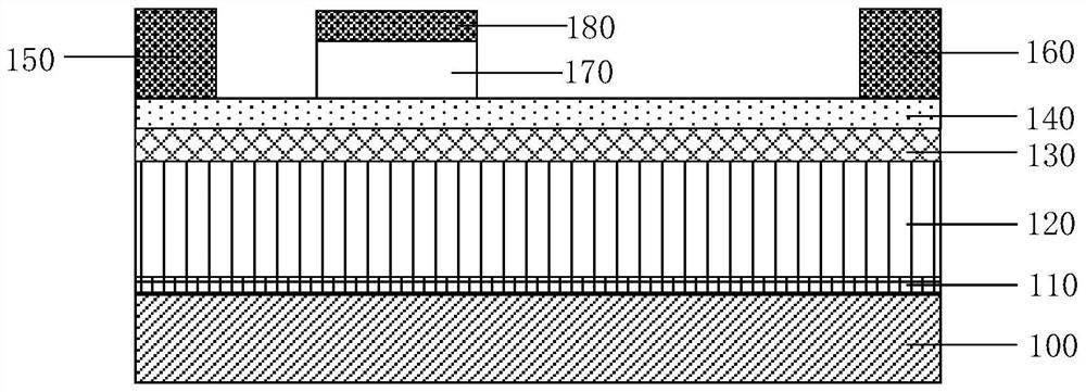
Using this technical means can take advantage of the good ohmic contact between the P-type GaN or P-type AlGaN layer and the metal gate. The charge in the gallium nitride layer is released quickly, which ensures the threshold stability of the device, but the ohmic gate contact essentially only exists by the P-type gallium nitride or P-type aluminum gallium nitride layer, the aluminum gallium nitride barrier layer and the nitride The PiN diode composed of a gallium channel layer, so when the gate voltage exceeds the turn-on voltage of the PiN diode, the gate current will increase rapidly, resulting in the normal operation of the device. The gate voltage does not exceed 3V, which makes the device subject to many restrictions in system use.

Method used


Image

  • Gallium nitride power semiconductor device with high threshold stability
  • Gallium nitride power semiconductor device with high threshold stability
  • Gallium nitride power semiconductor device with high threshold stability

Examples


Embodiment 1

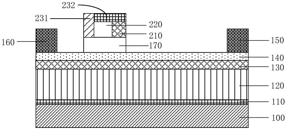
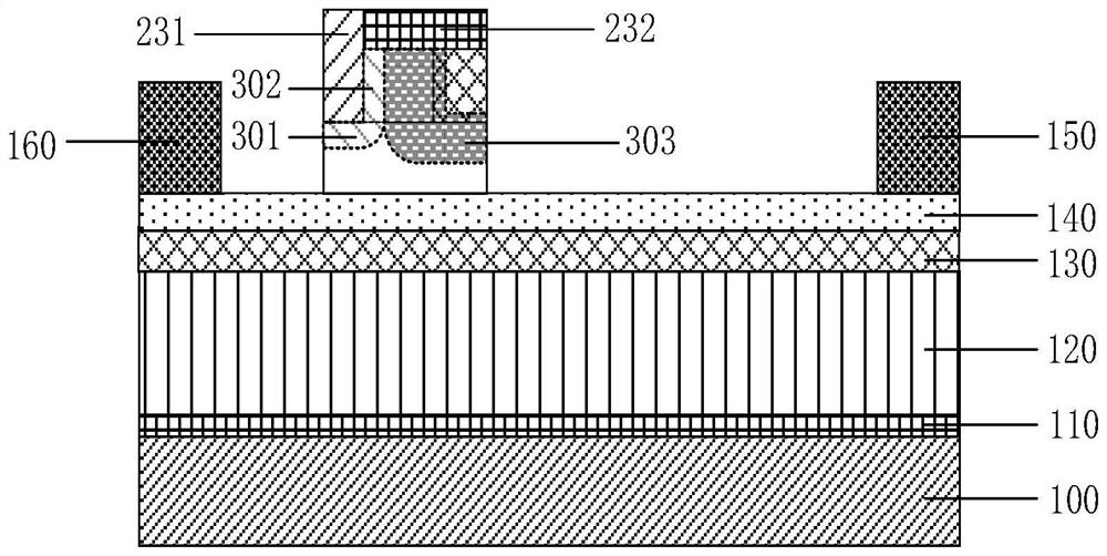
[0045] refer to figure 2 The shown GaN power semiconductor device with high threshold value stability is characterized in that it includes, from bottom to top: a substrate 100, a nucleation layer 110, a drift region 120, a channel layer 130, a potential The barrier layer 140, the first p-type gallium nitride cap layer 170, the metal source electrode 160, and the metal drain electrode 150 placed on the upper surface of the barrier layer 140 also include a second p-type gallium nitride cap layer 220, The sidewalls of the n-type gallium nitride cap layer 210 are in direct contact to form a pn junction, and both are placed on the upper surface of the first p-type gallium nitride cap layer 170 and have the same thickness; Schottky contact type metal gate electrode 231, disposed on the first p-type gallium nitride cap layer 170 and in contact with the sidewall of the second p-type gallium nitride cap layer 220, the Schottky metal gate electrode 231 is higher than the first p-type g...

Embodiment 2

[0049] refer to Figure 5 , compared with embodiment 1, the device described in this example is not provided with the second p-type gallium nitride cap layer 220 and the n-type gallium nitride cap layer on the first p-type gallium nitride cap layer 170 210. An ohmic metal gate electrode 232 and a Schottky metal gate electrode 231 are directly provided on the upper surface of the first p-type gallium nitride cap layer 170, and the Schottky metal gate electrode 231 is distributed on the on both sides of the ohmic metal gate electrode 232 . Other structures are the same as in Embodiment 1.

[0050] The advantages and gain effects achieved by Embodiment 1 are the same. Under high gate voltage, this embodiment has lower gate current. Under low gate voltage or zero gate voltage, the first p-type gallium nitride cap layer 170 or The potential of the potential barrier layer 140 is the same as that of the ohmic metal gate electrode 232, which eliminates the charge storage effect and ...

Embodiment 3

[0052] refer to Image 6 , compared with embodiment 2, in the device gate structure described in this example, a second p-type gallium nitride cap layer 220 is provided in the middle of the upper surface of the first p-type gallium nitride cap layer 170, and the second p-type gallium nitride cap layer 220 is The doping concentration of the gallium nitride cap layer 220 may be lower than that of the first p-type gallium nitride cap layer 170, and the two sides of the second p-type gallium nitride cap layer 220 are provided with Schottky metal gate electrodes 231, and the Schottky metal gate electrode 231 is in contact with the upper surface of the first p-type gallium nitride cap layer 170 to form a Schottky junction, and in contact with the sidewall of the second p-type gallium nitride cap layer 220 to form a Schottky junction, the upper surface of the second p-type gallium nitride cap layer 220 is provided with an ohmic metal gate electrode 232 .

[0053] The advantages and ...


PUM

PropertyMeasurementUnit
widthaaaaaaaaaa
widthaaaaaaaaaa

Abstract

The invention discloses a gallium nitride power semiconductor device with high threshold stability, which comprises a substrate, a nucleating layer, a drift region, a channel layer, a barrier layer, afirst p-type gallium nitride cap layer, a metal source electrode and a metal drain electrode; the upper surface of the first p-type gallium nitride cap layer is provided with a second p-type galliumnitride cap layer, an n-type gallium nitride cap layer and a Schottky contact type metal gate electrode, and the upper surfaces of the second p-type gallium nitride cap layer and the n-type gallium nitride cap layer are provided with ohmic contact type metal gate electrodes; and the Schottky contact type metal gate electrode is in direct contact with the side wall of the ohmic contact type metal gate electrode. According to the invention, the charge storage phenomenon can be effectively eliminated under low gate voltage, and the device is ensured to have higher threshold stability under the working condition of repeated switching; therefore, the gate leakage of the device can be reduced under high gate voltage, and the device is ensured to have a long-term stable working state under high gate voltage.

Description

technical field [0001] The invention mainly relates to the field of power semiconductor devices, in particular, a gallium nitride power semiconductor device with high threshold value stability. Background technique [0002] Gallium nitride (GaN), as a representative of the third-generation semiconductor, has the characteristics of large band gap, high electron saturation drift velocity, high critical breakdown electric field, high thermal conductivity and small dielectric constant. Wide bandgap and high breakdown electric field strength can greatly increase the peak voltage that the device can withstand and increase the output power of the device; high electron saturation drift rate enables the device to adapt to higher operating frequencies; high thermal conductivity enables the device to withstand higher temperature, thus greatly improving the stability and reliability of the system. Among them, the high electron mobility transistor (HEMT) prepared by the two-dimensional ...

Claims


Application Information

Patent Timeline
Patent Type & Authority Applications(China)
IPC IPC(8): H01L29/778
CPCH01L29/7786
Inventor 刘斯扬张弛辛树轩李胜钱乐葛晨孙伟锋时龙兴
Owner SOUTHEAST UNIV
Learn More