Opto-electronic device having a light-emitting diode and a light sensor

a technology of light-emitting diodes and opto-electronic devices, which is applied in the direction of radiation controlled devices, optical radiation measurement, instruments, etc., can solve the problems of limited miniaturization, high manufacturing cost, and inability to meet the requirements of large-scale production, and achieves easy large-scale production, low manufacturing cost, and simplified manufacturing

Inactive Publication Date: 2006-05-04
FRAUNHOFER GESELLSCHAFT ZUR FOERDERUNG DER ANGEWANDTEN FORSCHUNG EV
View PDF5 Cites 14 Cited by
  • Summary
  • Abstract
  • Description
  • Claims
  • Application Information

AI Technical Summary

Benefits of technology

[0023] One advantage of the present invention is that the opto-electronic device may be manufactured with low manufacturing expense and thus easily in large numbers. In particular, the manufacturing of the inventive opto-electronic device requires no generation of a recess as it is required according to the prior art. The manufacturing of the inventive opto-electronic device is thus performed using known and well-controlled semiconductor technologies and using available devices or available equipment, respectively.
[0024] The manufacturing is simplified by the fact that it requires no generation of a metallization in a recess. Further, any process steps for generating, metallizing and passivating a recess are omitted.
[0025] For contacting the light-emitting diode, preferably conductive traces are used. Bond wires are not required. Compared to the prior art, in the manufacturing of the inventive opto-electronic device any working steps for mounting the SMD light-emitting diode are omitted.
[0026] The lateral precision of the manufacturing and the arrangement of the light-emitting diode correspond to the accuracy of a semiconductor manufacturing process. This is typically below the micrometer scale and is thus better by a factor of 10 to 100 than in the conventionally required mounting of the SMD light-emitting diode whose lateral position inaccuracy is always several 10 μm. Further, steps for the adjustment or calibration of the mounting position of the conventional SMD light-emitting diode 16 are omitted.
[0027] It is a further advantage of the present invention that the building height of a light-emitting diode having a light-emitting layer of an organic material comprising 150 nm to 160 nm is extremely small. The organic light-emitting diode is thus thinner than passivation layers across conductive traces of a semiconductor chip.
[0028] A further important advantage of the present invention is that the opto-electronic device is completed fully on wafer level or before dicing. The opto-electronic device may thus be tested in the wafer arrangement which enables a cost-effective manufacturing, in particular with large numbers.

Problems solved by technology

With regard to manufacturing technology, this realization is very expensive, however.
Further, a miniaturization is only restrictedly possible even when using surface-mounted devices.
One disadvantage of the conventional opto-electronic device illustrated with reference to FIG. 2 is that the generation of the pit or recess 14, respectively, requires special or additional process steps, respectively.
This increases the manufacturing costs and, like every process step, the probability of a defect, and thus the waste material of the production.
A further disadvantage is that a metallization or the generation of a conductive trace in the recess 14, respectively, is, for example, critical for contacting the side of the SMD light-emitting diode 16 facing the Si substrate 10.

Method used


Image

  • Opto-electronic device having a light-emitting diode and a light sensor
  • Opto-electronic device having a light-emitting diode and a light sensor
  • Opto-electronic device having a light-emitting diode and a light sensor

Examples


Embodiment Construction

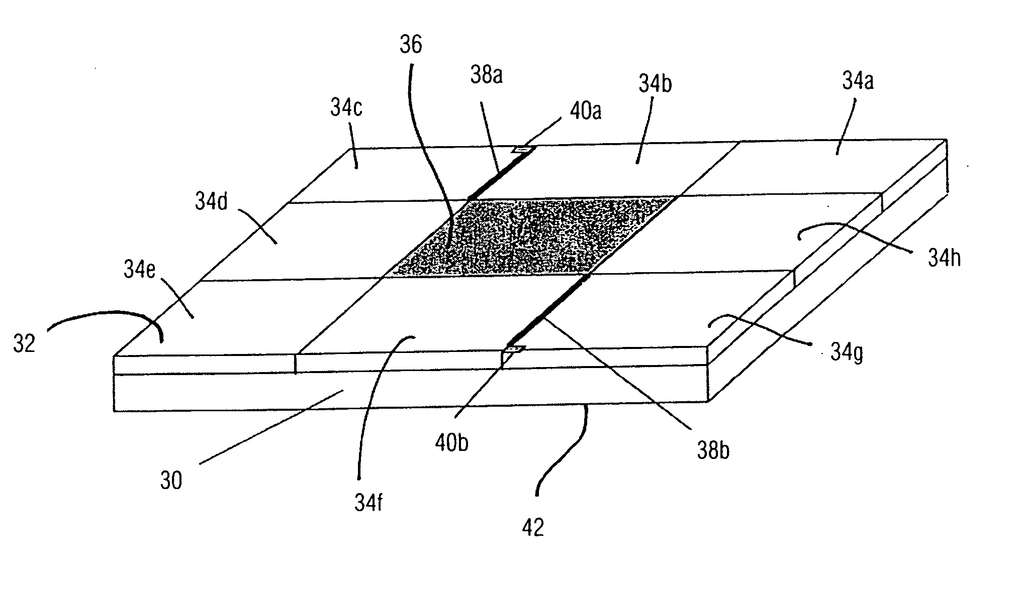
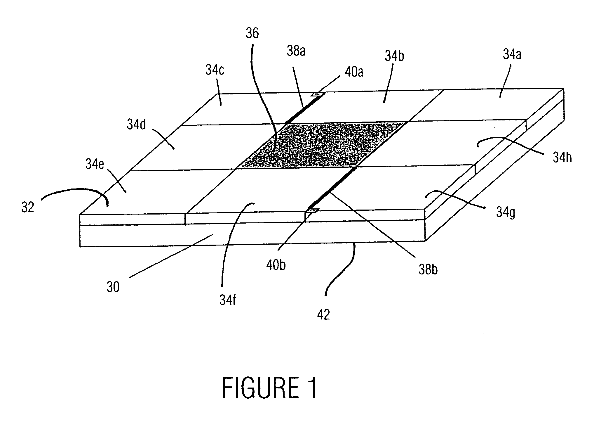
[0036]FIG. 1 is a schematic illustration of a perspective view of an opto-electronic device according to a preferred embodiment of the present invention. An Si substrate 30 comprises eight light sensors 34a, . . . , 34h and a light-emitting diode 36 on one surface 32. The light sensors 34a, . . . , 34h and the light-emitting diode 36 respectively comprise a substantially rectangular or square shape. The light sensors 34a, . . . , 34h and the light-emitting diode 36 are arranged in a grid-like shape of three rows lying next to each other respectively having three devices, wherein the light-emitting diode 36 is in the middle and is surrounded by the light sensors 34a, . . . , 34h on all sides. The light sensors 34a, . . . , 34h are preferably semiconductor light sensors, for example photodiodes, phototransistors, photoresistive devices or other photosensitive devices having an electrical characteristic which is changed by incoming light in a known way.

[0037] The light-emitting diode ...


PUM


Abstract

An opto-electronic device includes a substrate, a light sensor and a light-emitting diode having a light-emitting layer of an organic material, wherein the light sensor and the light-emitting diode are monolithically integrated with the substrate.

Description

CROSS-REFERENCE TO RELATED APPLICATIONS [0001] This application is a continuation of co-pending International Application No. PCT / EP2003 / 005253, filed May 19, 2003, which designated the United States and was not published in English. BACKGROUND OF THE INVENTION [0002] 1. Field of the invention [0003] The present invention relates to an opto-electronic device having a light-emitting diode and a light sensor in particular usable for detecting a path length, an angle of rotation, a distance or a position, and to a method for manufacturing the same. [0004] 2. Description of the Related Art [0005] In numerous fields of the art, opto-electronic devices or systems, respectively, are used to detect distances, path lengths, angles of rotation, positions and other variables. To this end, in particular opto-electronic devices are used which include a light source or radiation source, respectively, and a light sensor or a light-sensitive detector, respectively. [0006] Light emitted from the lig...

Claims


Application Information

Patent Timeline
Patent Type & Authority Applications(United States)
IPC IPC(8): G01J1/42H01L27/144H01L27/30H01L31/12H01L31/153H01L31/173H01L31/18
CPCH01L27/1446H01L27/30H01L31/125H01L31/153H01L31/173H01L31/18H01L2224/48472H01L2224/48091H01L2924/00014H01L2924/3011H01L2924/00H01L2924/10253H01L2924/12044H10K39/00
Inventor GRUEGER, HEINRICHSCHNEIDER, TORSTENAMELUNG, JOERGSAUER, BODO
Owner FRAUNHOFER GESELLSCHAFT ZUR FOERDERUNG DER ANGEWANDTEN FORSCHUNG EV
Why Eureka
Try Eureka