Boron phosphide-based semiconductor light-emitting device and production method thereof

light-emitting device technology, which is applied in the direction of semiconductor devices, basic electric elements, electrical appliances, etc., can solve the problems of failure to achieve the diffusion of the device operation current widely in a light-emitting area, failure to achieve the emission intensity of a boron phosphide-based semiconductor light-emitting device to be fully attained, and failure to completely complete the effect of complete failur

Inactive Publication Date: 2006-07-27
SHOWA DENKO KK
View PDF14 Cites 11 Cited by
  • Summary
  • Abstract
  • Description
  • Claims
  • Application Information

AI Technical Summary

Benefits of technology

The patent describes a new type of semiconductor light-emitting device made with boron phosphide. The device has a high-resistance layer made of boron phosphide with a resistivity of 10 Ω·cm or higher. This results in improved performance and efficiency of the device.

Problems solved by technology

The technical problem addressed in this patent is the short circuit of an electric current in a boron phosphide-based semiconductor light-emitting device, which limits the attainment of increased emission intensity. The invention provides a pad electrode that effectively diffuses the device operation current in a wide range of an emission area to overcome this problem.

Method used


Image

  • Boron phosphide-based semiconductor light-emitting device and production method thereof
  • Boron phosphide-based semiconductor light-emitting device and production method thereof
  • Boron phosphide-based semiconductor light-emitting device and production method thereof

Examples


example 1

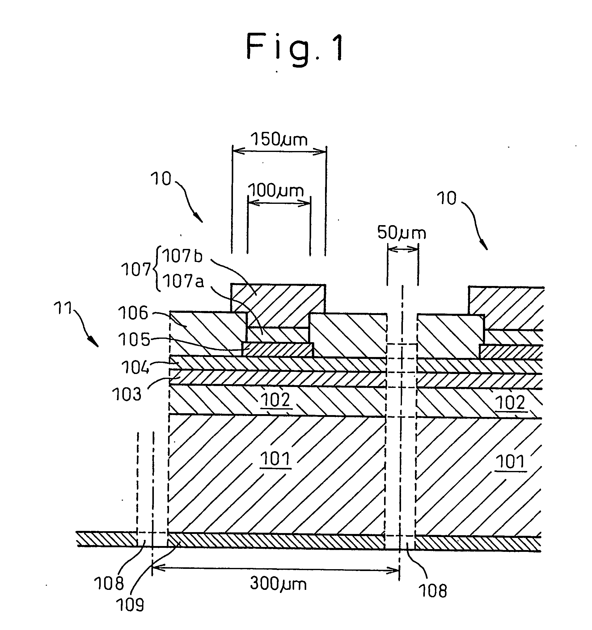
[0069] The boron phosphide-based compound semiconductor light-emitting device according to the present invention will next be described in detail, taking as an example a light-emitting diode (LED) employing a pad electrode having a bottom surface which is in contact with a high-resistance boron phosphide amorphous layer. FIG. 1 schematically shows the cross-section of a stacked structure 11 employed for fabricating an LED 10 having a double-hetero (DH) structure.

[0070] A phosphorus (P)-doped n-type silicon (Si) single crystal was used as a substrate 101. On the surface of the substrate 101, a lower cladding layer 102 formed of n-type boron phosphide (BP) was deposited through use of atmospheric pressure (near atmospheric pressure) metal-organic vapor phase epitaxy (MOVPE) means. The lower cladding layer 102 was deposited at 950° C. by use of a triethylboran (molecular formula: (C2H5)3B) as a boron (B) source and phosphine (molecular formula: PH3) as a phosphorus source. The carrier...

example 2

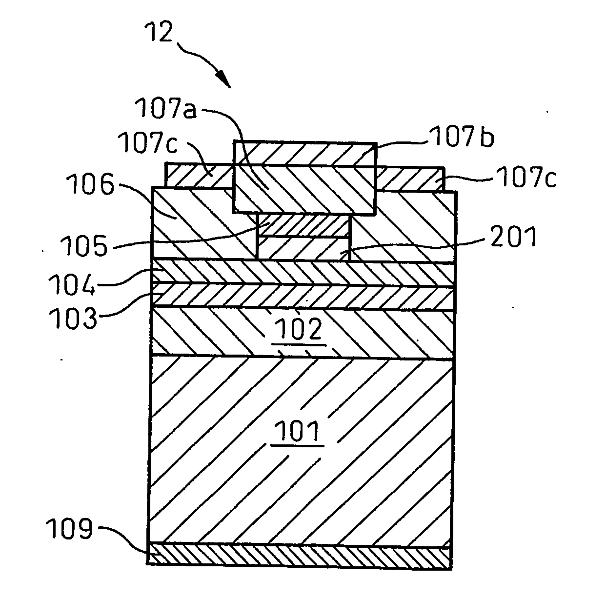
[0079] The boron phosphide-based compound semiconductor light-emitting device according to the present invention will next be described in detail, taking as an example a double-heterojunction (DH) light-emitting diode (LED) employing a pad electrode having a bottom surface which is in contact with the surface of a boron phosphide amorphous layer of a multi-layer structure.

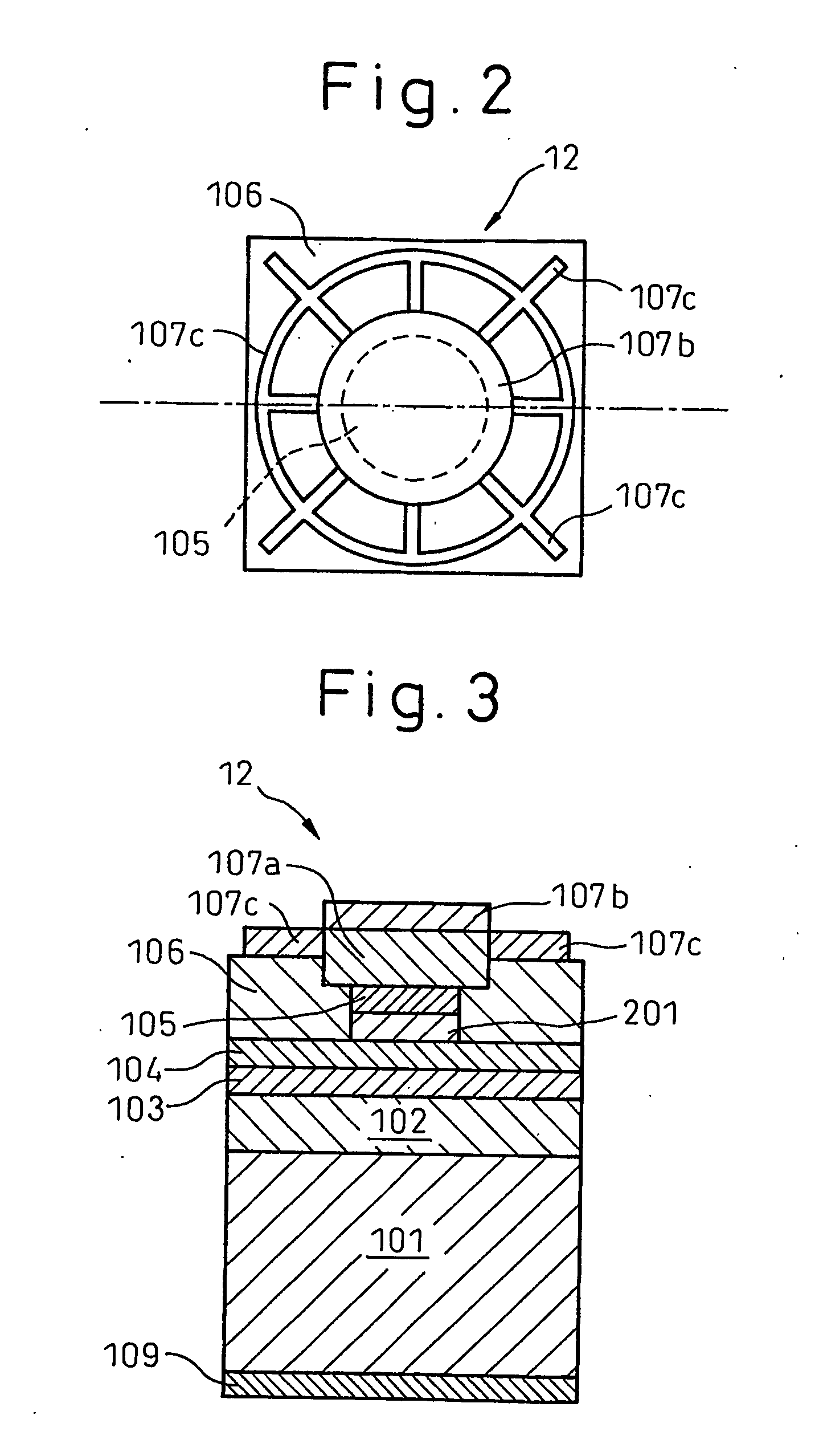
[0080]FIG. 2 is a schematic plane view of the LED 12 according to Example 2. FIG. 3 schematically shows a cross-section of the LED 12 taken along the broken line A-A′ shown in FIG. 2. In FIGS. 2 and 3, the same members as shown in FIG. 1 are denoted by the same reference numerals.

[0081] On an n-type GaN light-emitting layer 104 which had been formed in the same manner as described in Example 1, an undoped p-type boron phosphide amorphous layer 201 was formed. The carrier concentration and the thickness of the p-type boron phosphide amorphous layer 201 were controlled to 8×1018 cm−3 and 12 nm, respectively. On the...


PUM


Abstract

A boron phosphide-based semiconductor light-emitting device, comprising: a crystalline substrate; a first semiconductor layer formed on said crystalline substrate, said first semiconductor layer including a light-emitting layer, serving as a base layer and having a first region and a second region different from the first region; a boron phosphide-based semiconductor amorphous layer formed on said first region of said first semiconductor layer, said boron phosphide-based semiconductor amorphous layer including a high-resistance boron phosphide-based semiconductor amorphous layer or a first boron phosphide-based semiconductor amorphous layer having a conduction type opposite to that of said first semiconductor layer; a pad electrode formed on said high-resistance or opposite conductivity-type boron phosphide-based semiconductor amorphous layer for establishing wire bonding; and a conductive boron phosphide-based crystalline layer formed on said second region of said first semiconductor layer, said conductive boron phosphide-based crystalline layer extending optionally to a portion of said boron phosphide-based semiconductor amorphous layer, wherein said pad electrode is in contact with said boron phosphide-based semiconductor crystalline layer at a portion of said pad electrode above the bottom of said pad electrode.

Description


Claims


Application Information

Patent Timeline
Owner SHOWA DENKO KK
Why Eureka
Try Eureka