Semiconductor device including resistor and method of fabricating the same

Inactive Publication Date: 2006-08-31
SAMSUNG ELECTRONICS CO LTD
View PDF14 Cites 11 Cited by
  • Summary
  • Abstract
  • Description
  • Claims
  • Application Information

AI Technical Summary

Benefits of technology

[0025] In another embodiment, after forming the upper resistor pattern, insulating spacers may be formed to cover sidewalls of the upper resistor pattern. Further, highly doped layers which are doped with impurity ions of

Problems solved by technology

However, in the case of a resistor, which is a passive element, there is a limit in reducing the scale of the resistor so as to satisfy a large resistance value required for

Method used


Image

  • Semiconductor device including resistor and method of fabricating the same
  • Semiconductor device including resistor and method of fabricating the same
  • Semiconductor device including resistor and method of fabricating the same

Examples


Embodiment Construction

[0036] The present invention will now be described more fully hereinafter with reference to the accompanying drawings, in which preferred embodiments of the invention are shown. This invention may, however, be embodied in different forms and should not be construed as limited to the embodiments set forth herein. In the figures, if a layer is described as being “on” another layer or a substrate, the layer can be formed directly on another layer or a substrate, or another layer can be interposed therebetween. Like numbers refer to like elements throughout the specification.

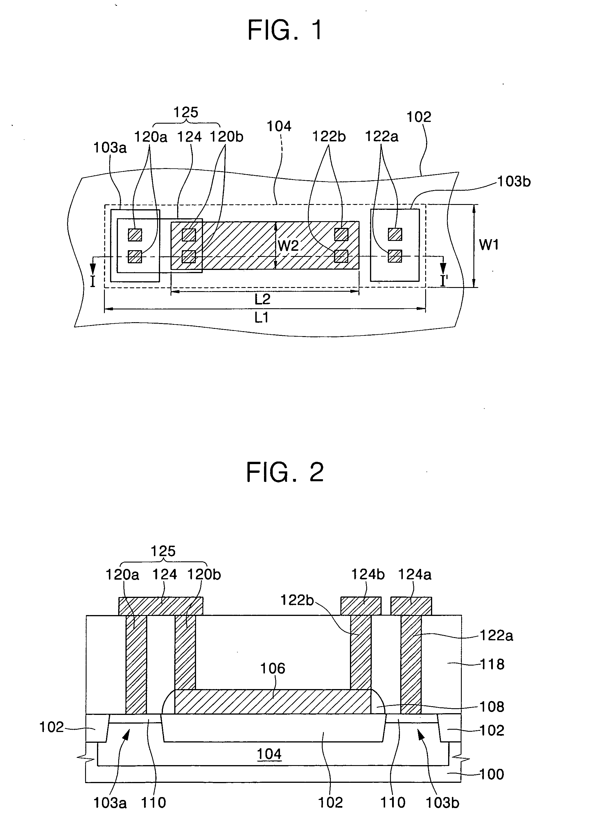
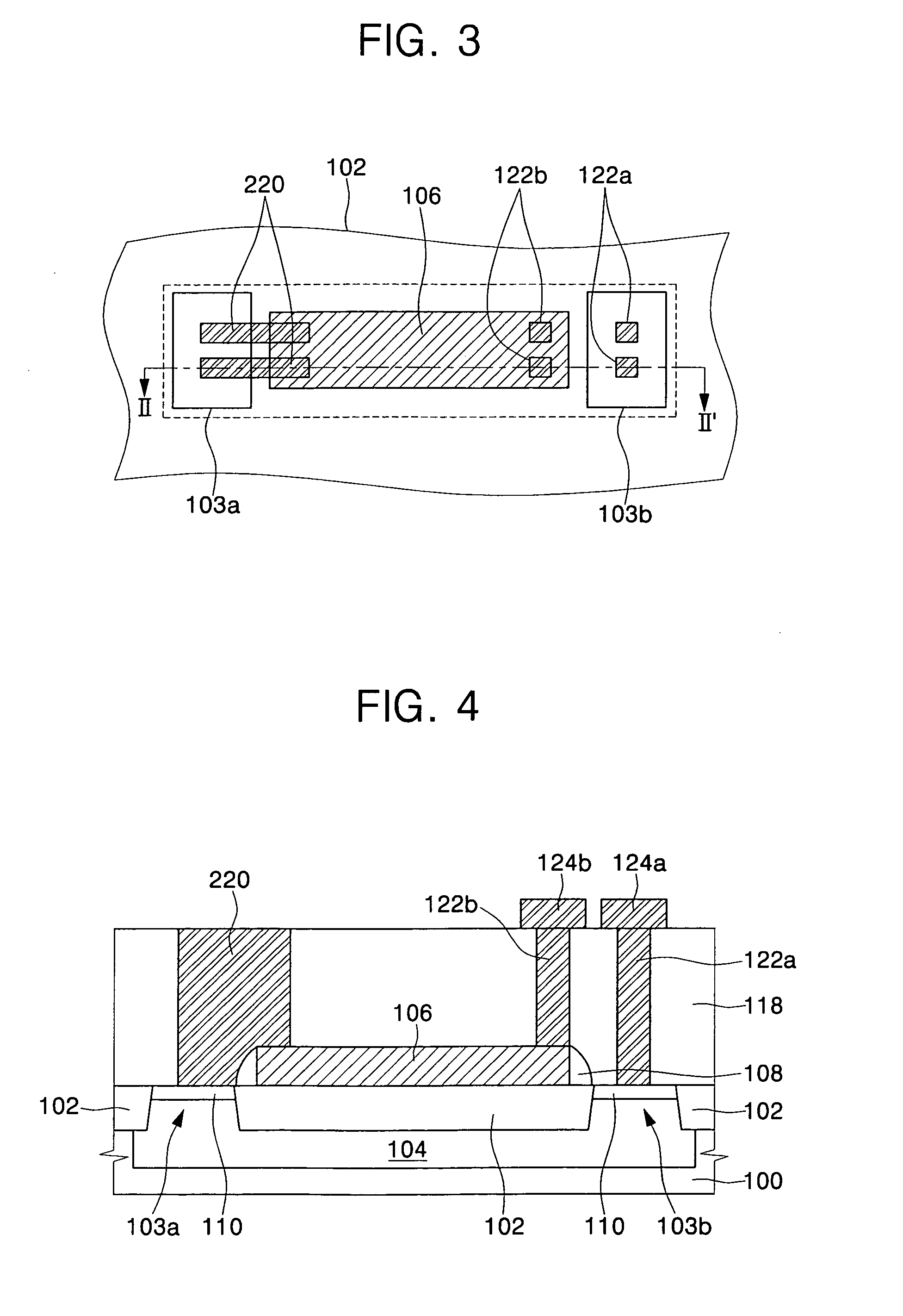
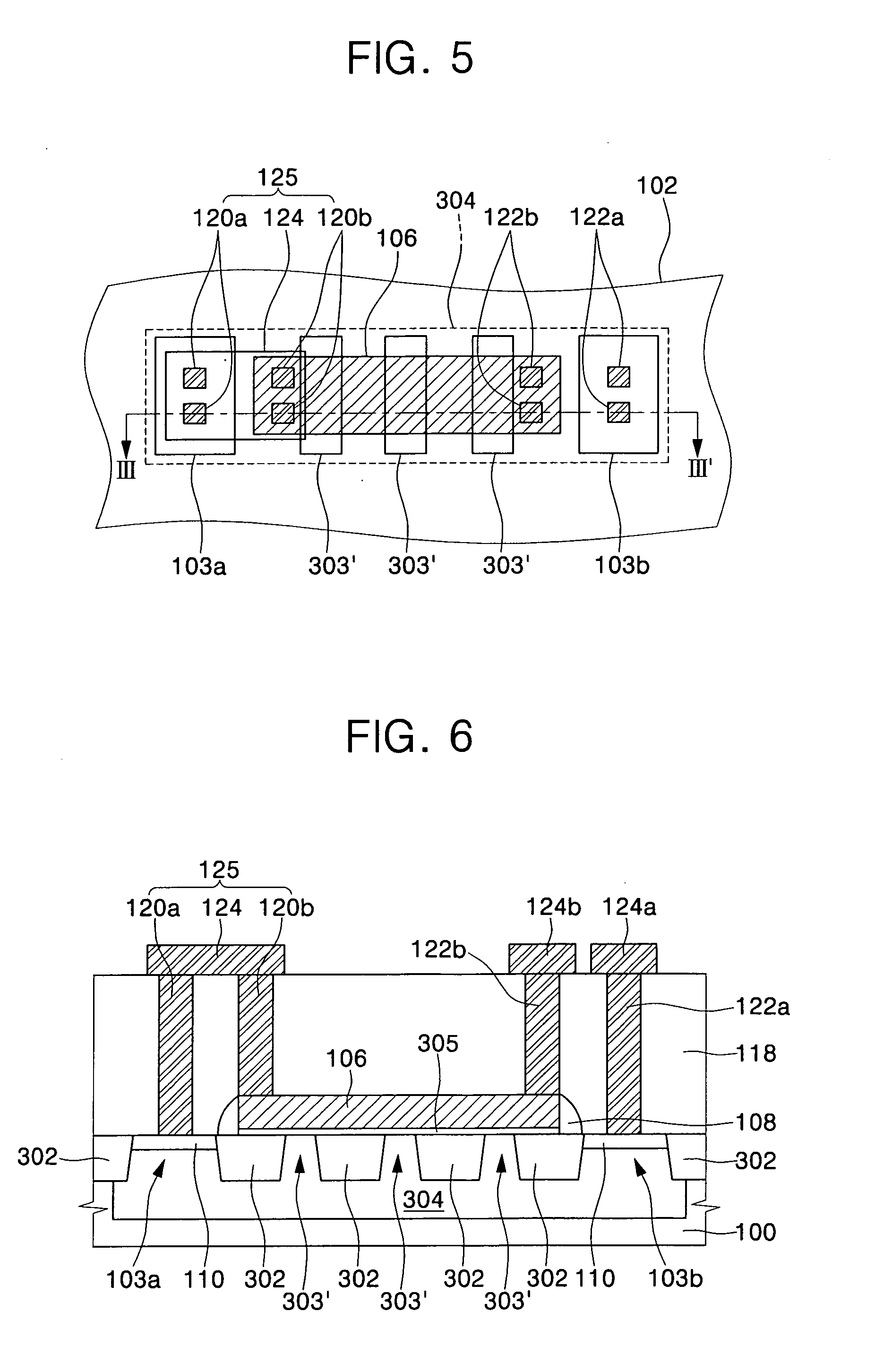
[0037]FIG. 1 is a plan view of a semiconductor device including a resistor according to an embodiment of the present invention, and FIG. 2 is a cross-sectional view taken along line I-I′ shown in FIG. 1.

[0038] Referring to FIGS. 1 and 2, an isolation insulating layer 102 is disposed in a semiconductor substrate 100. The isolation insulating layer 102 defines at least two active regions 103a and 103b spaced apart f...


PUM


Abstract

In a semiconductor device including a resistor and a method of fabricating the same, the semiconductor device includes an isolation insulating layer disposed in a semiconductor substrate to define at least two active regions spaced from each other. A well resistor pattern is disposed below the isolation insulating layer to connect the active regions. An upper resistor pattern is disposed on the isolation insulating layer between the active regions. A resistor connector electrically connects a selected one of the active regions with the upper resistor pattern so that the well resistor pattern and the upper resistor pattern are connected in series.

Description

RELATED APPLICATIONS [0001] This application claims the priority of Korean Patent Application No. 2005-0016824, filed on Feb. 28, 2005, in the Korean Intellectual Property Office, the disclosure of which is incorporated herein in its entirety by reference. BACKGROUND OF THE INVENTION [0002] 1. Field of the Invention [0003] The present invention relates to a semiconductor device and a method of fabricating the same, and more particularly, to a semiconductor device including a resistor having a sufficient resistance value while achieving high integration and a method of fabricating the same. [0004] 2. Description of the Related Art [0005] Semiconductor memory devices commonly include a cell region in which a plurality of unit cells are arranged at regular intervals and a peripheral region which is located adjacent to the cell region and drives and controls the unit cells. In the peripheral region, transistors, diodes, and resistors, which drive the unit cells, are formed. [0006] Conve...

Claims


Application Information

Patent Timeline
IPC IPC(8): H01L21/302
CPCH01L27/08H01L29/8605B67D7/04B67D7/06F16K17/02F16L11/04
Inventor OH, MYOUNG-HWANKANG, HEE-SUNGRYOU, CHOONG-RYUL
Owner SAMSUNG ELECTRONICS CO LTD
Why Eureka
Try Eureka