Semiconductor device and fabrication method of semiconductor device

a semiconductor device and semiconductor technology, applied in the direction of semiconductor devices, basic electric elements, electrical appliances, etc., can solve the problems of affecting the operation of the original semiconductor device, the operation of the parasitic element is likely to be abnormal, and the semiconductor device may exceed the safe operation rang

Active Publication Date: 2011-08-25
DENSO CORP +1
View PDF5 Cites 7 Cited by
  • Summary
  • Abstract
  • Description
  • Claims
  • Application Information

AI Technical Summary

Benefits of technology

[0014]It is an object of the present invention to at least solve the above problems in the conventional technologies.
[0015]According to one aspect of the present invention, a semiconductor device includes a first semiconductor region of a first conductivity type; a second semiconductor region of a second conductivity type, disposed on a surface of the first semiconductor region, and having an impurity concentration higher than that of the first semiconductor region; a trench that penetrates the second semiconductor region to reach the first semiconductor region; a first electrode disposed inside the trench via an insulating film; a first recess portion disposed deeper than an upper end of the first electrode, in a surface layer of the second semiconductor region, so as to be in contact with the trench; and a second electrode embedded in the first recess portion.

Problems solved by technology

However, in conventional insulated gate semiconductor devices such as MOSFET and IGBT, a parasitic element such as a parasitic bipolar transistor and a parasitic thyristor are incidentally formed in addition to original constituent elements of the semiconductor devices.
Such a parasitic element is likely to operate at abnormal times such as when an overcurrent flows in the semiconductor devices.
It is problematic that the operation of the parasitic element adversely affects the operation of the original semiconductor devices.
Therefore, destruction may occur if the semiconductor device exceeds a safe operation range.
However, a semiconductor device fabricated in this way becomes unable to sufficiently invert the channel region in the on-state.
Therefore, the on-voltage problematically increases.
Such a problem also occurs in IGBT of the trench gate structure.

Method used


Image

  • Semiconductor device and fabrication method of semiconductor device
  • Semiconductor device and fabrication method of semiconductor device
  • Semiconductor device and fabrication method of semiconductor device

Examples


first embodiment

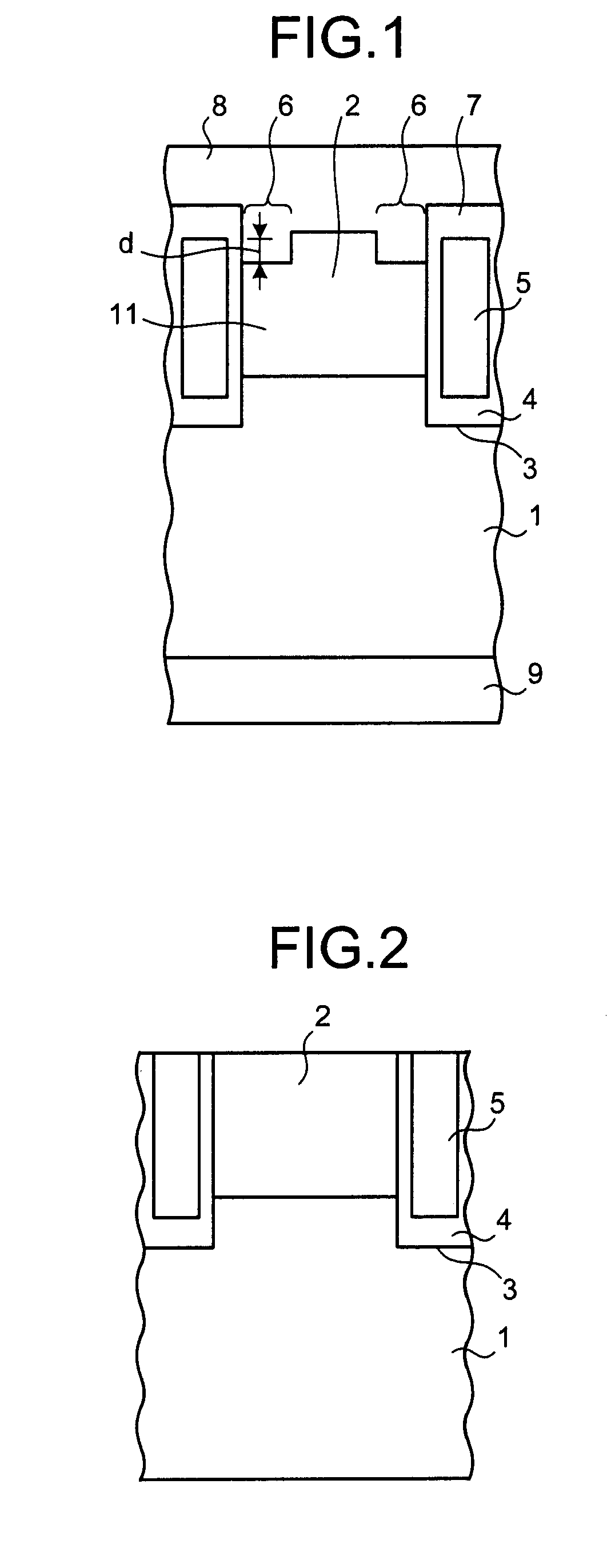
[0030]A method of fabricating such a semiconductor device will be described. FIGS. 2 to 5 are cross-sectional views of a semiconductor device and depict a fabrication method thereof according to the First, as depicted in FIG. 2, the p-type base region 2 is laid by an epitaxial growth method, for example, on the surface of the semiconductor substrate forming the n−-type drift region 1. For example, photolithography is used for forming the trench 3 that penetrates the base region 2 to reach the drift region 1. The gate insulating film 4 made up of a thin silicon dioxide film (SiO2) is then formed on the side surface and the bottom surface of the trench 3 by a thermal oxidation method, for example. The gate electrode 5 is formed inside the trench 3 via the gate insulating film 4 by embedding polysilicon (Poly-Si), for example.

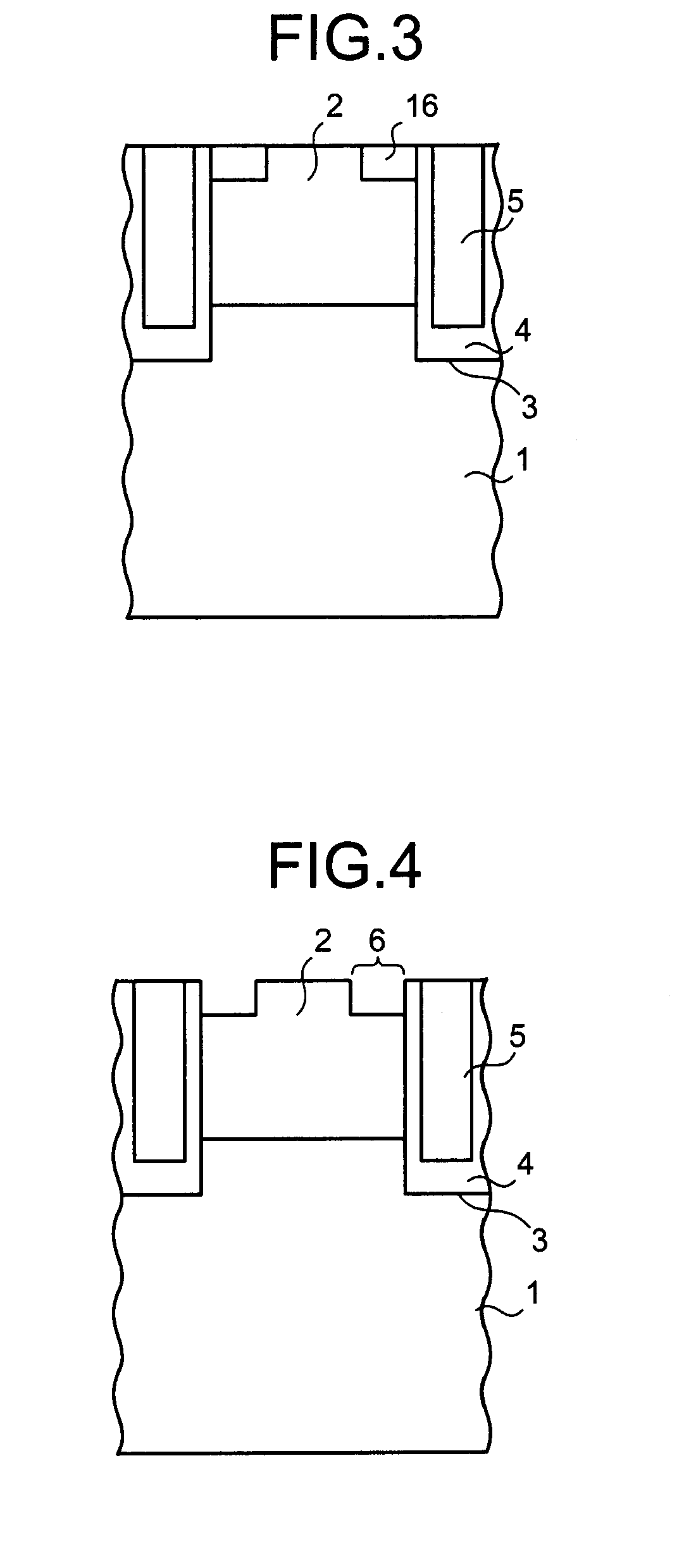
[0031]As depicted in FIG. 3, an impurity region 16 is then formed in the surface layer of the base region 2 by introducing an impurity into a region deeper than ...

fourth embodiment

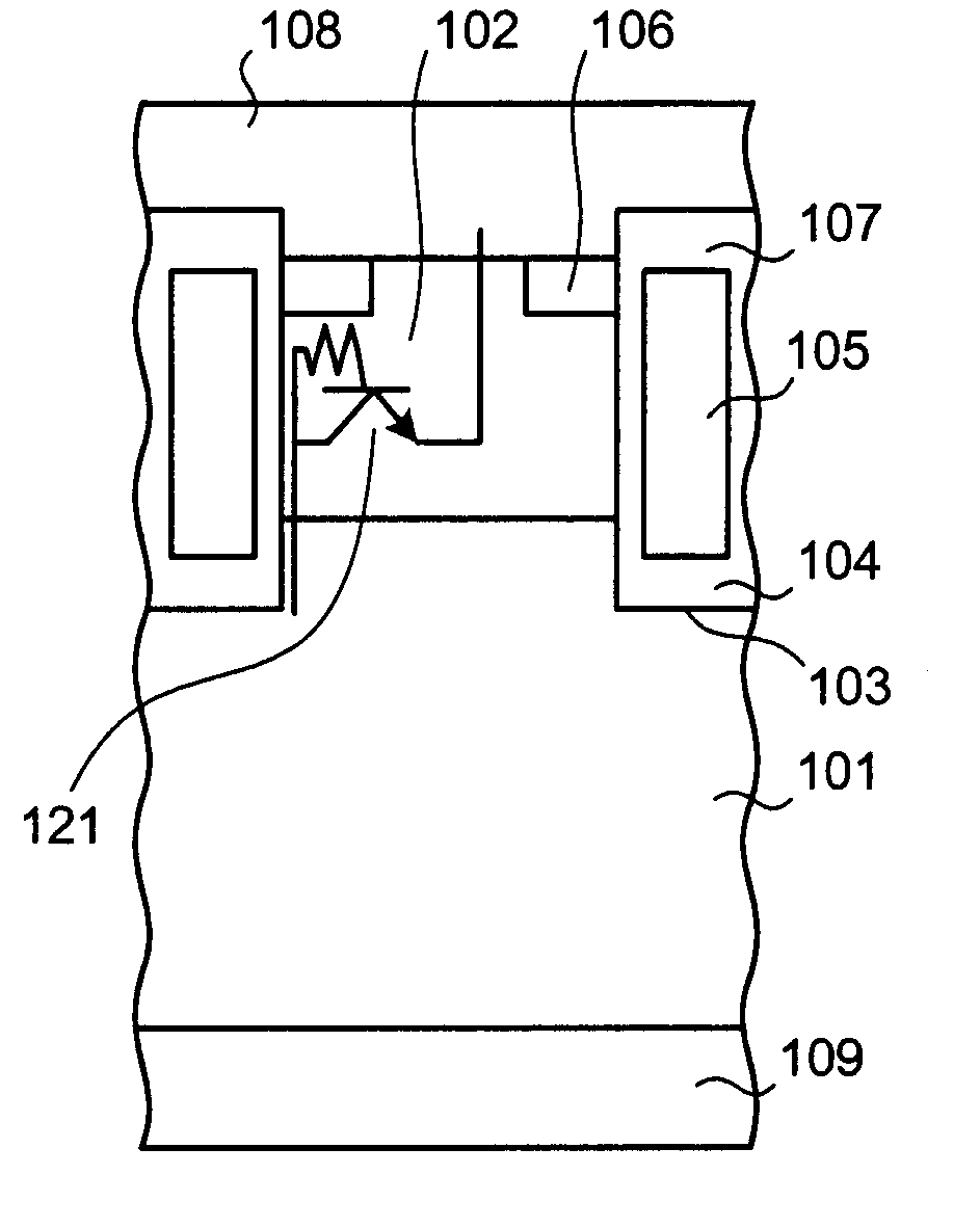
[0043]FIG. 10 is a cross-sectional view of a semiconductor device according to a In the semiconductor device depicted in FIG. 10, a p-type base region 22 is selectively disposed on a surface layer of a semiconductor substrate acting as an n−-type drift region 21. The base region 22 has an impurity concentration higher than that of the drift region 21. The drift region 21 corresponds to a first semiconductor region. The base region 22 corresponds to a second semiconductor region.

[0044]A second recess portion 26 is formed in the surface layer of the base region 22. Therefore, the base region 22 has an uneven surface shape made up of the first recess portion 6 and a protruding portion without the first recess portion 6. In the surface of the semiconductor substrate, a gate electrode 25 is disposed via a gate insulating film 24 to cover the protruding portion of the base region 22 and to project into the second recess portion 26. Therefore, the second recess portion 26 is disposed to o...


PUM


Abstract

A semiconductor device includes a first semiconductor region of a first conductivity type; a second semiconductor region of a second conductivity type, disposed on a surface of the first semiconductor region, and having an impurity concentration higher than that of the first semiconductor region; a trench that penetrates the second semiconductor region to reach the first semiconductor region; a first electrode disposed inside the trench via an insulating film; a first recess portion disposed deeper than an upper end of the first electrode, in a surface layer of the second semiconductor region, so as to be in contact with the trench; and a second electrode embedded in the first recess portion.

Description

BACKGROUND OF THE INVENTION[0001]1. Field of the Invention[0002]The present invention relates to a semiconductor device and fabrication method thereof.[0003]2. Description of the Related Art[0004]For electric power converting apparatuses used in electric vehicles (EV), etc., the most widely used insulated gate semiconductor devices have lower power consumption and are easily driven in a voltage-controlled manner. Insulated gate semiconductor devices are known as an insulated gate field effect transistor (metal oxide semiconductor field effect transistor (MOSFET)), an insulated gate bipolar transistor (IGBT), etc.[0005]In the present description and the accompanying drawings, “n” and “p” prefixes of layers and regions indicate that the majority of carriers is an electron and a hole, respectively. “+” and “−” appended to an “n” or a “p” indicate that the impurity concentration is higher and lower, respectively, than layers and regions without “+” and “−”.[0006]FIG. 6 is a cross-sectio...

Claims


Application Information

Patent Timeline
Patent Type & Authority Applications(United States)
IPC IPC(8): H01L29/41H01L21/76
CPCH01L29/41766H01L29/66348H01L29/66727H01L29/7813H01L29/7397H01L29/7802H01L29/66734
Inventor MOMOTA, SEIJIFUJII, TAKESHIKAMIJIMA, SATOSHIASAI, MAKOTO
Owner DENSO CORP
Why Eureka
Try Eureka