Imaging device

a technology of optical carriers and optical carriers, applied in the field of optical carriers, can solve the problems of increasing leak current due to crystal defects, increasing the number of crystal defects, so as to and improve the transfer efficiency of optical carriers. the effect of crystal defects at the surface of the first diffusion region

Inactive Publication Date: 2008-02-07
SOCIONEXT INC
View PDF15 Cites 7 Cited by
  • Summary
  • Abstract
  • Description
  • Claims
  • Application Information

AI Technical Summary

Benefits of technology

[0016] In a preferred example in the second aspect of the imaging device of the present invention, a third diffusion region is formed in the peripheral part on the gate electrode side of the first diffusion region at the surface of the first diffusion region. The third diffusion region is of the first conductive type and has an impurity concentration higher than an impurity concentration of the first diffusion region. When crystal defects do not tend to occur at the surface of the first diffusion region adjacent to the gate electrode in the process of forming the gate electrode, the transfer efficiency of the optical carriers stored in the first diffusion region can be further improved if the third diffusion region is formed at the surface near a channel region of the transfer transistor in the first diffusion region.
[0017] In a preferred example in the second aspect of the imaging device of the present invention, a plurality of third diffusion regions is sequentially formed toward the gate electrode inside the second diffusion region in an inner part of and at the surface of the first diffusion region. The third diffusion regions are of the first conductive type and have impurity concentrations higher than an impurity concentration of the first diffusion region. The nearer the gate electrode, the higher the impurity concentration of the third diffusion region becomes. In this case, a built-in potential gradient can be formed toward the gate electrode side. In other words, electrons being optical carriers can be sequentially moved to the diffusion regions close to the gate electrode, which can improve the transfer efficiency of the optical carriers stored in the first diffusion region.
[0018] In a third aspect of the imaging device of the present invention, a pixel which receives relatively short-wavelength light incident via a first filter has the same structure as in the above first aspect. A pixel which receives relatively long-wavelength light incident via a second filter has a second diffusion region which is formed to cover an entire surface of the first diffusion region. By covering the entire surface of the first diffusion region with the second diffusion region, crystal defects at the surface of the first diffusion region can be reduced, which can reduce the dark current noise.
[0019] In a semiconductor of silicon or the like, a transmittance of the long-wavelength light is higher compared to a transmittance of the short-wavelength light. Therefore, in the pixel which receives the long-wavelength light, the light detection sensitivity does not tend to lower even if the entire surface of the first diffusion region is covered with the second diffusion region. On the other hand, the transmittance of the short-wavelength light is relatively low. Therefore, the pixel which receives the short-wavelength light is constituted by the first diffusion region having a region not covered with the second diffusion region to increase the light detection sensitivity. By changing the area of the second diffusion region according to the wavelength of incident light, the light detection sensitivity can be made uniform independently of wavelength while the occurrence of the dark current noise is minimized. For example, in the first diffusion region of each pixel receiving the relatively short-wavelength light, the area of a region exposed at the surface is made larger than the area of a region covered with the second diffusion region, which can improve the detection sensitivity of the photodiode while keeping the dark current noise to a minimum.
[0020] In a fourth aspect of the imaging device of the present invention, a pixel which receives relatively short-wavelength light incident via a first filter has the same structure as in the above second aspect. A pixel which receives relatively long-wavelength light incident via a second filter has a second diffusion region which is formed to cover an entire surface of the first diffusion region. Also in the fourth aspect, as in the above third aspect, the light detection sensitivity can be made uniform independently of wavelength while the occurrence of the dark current noise is minimized.
[0021] In a preferred example in the first to fourth aspects of the imaging device of the present invention, each pixel includes a reset transistor and a source follower transistor. A source electrode of the reset transistor is connected to the drain electrode of the transfer transistor and a drain electrode is connected to a voltage supply line. A gate electrode of the source follower transistor is connected to a floating diffusion node (the drain electrode of the transfer transistor and the source electrode of the reset transistor). The source follower transistor generates a pixel signal according to the amount of optical carriers and outputs the generated pixel signal from a source electrode. Since a contact region is not formed in the first diffusion region, any crystal defect in the first diffusion region does not occur due to the formation of the contact region. Accordingly, the occurrence of the dark current noise due to the formation of the contact region can be prevented.

Problems solved by technology

Since the peripheral part of the first diffusion region is close to an interelement isolation structure part, many crystal defects tend to exist therein.
Therefore, a leak current due to the crystal defects increases, and dark current noise tends to occur, so that in the peripheral part, a dark current larger than in a semiconductor surface of a central part of the first diffusion region occurs.
Further, when the gate electrode of the transistor is formed in the position adjacent to the first diffusion region, crystal defects sometimes occur in the peripheral part of the first diffusion region adjacent to the gate electrode due to the influence of stress in a process of forming the gate electrode.
There are many crystal defects near the isolation region where the periodicity of crystals of silicon or the like is destroyed.
Therefore, the nearer the isolation region, the more frequently the leak current which causes the dark current noise tends to occur.
There are many crystal defects near the isolation region where the periodicity of crystals of silicon or the like is destroyed.
Therefore, the nearer the isolation region, the more frequently the leak current which causes the dark current noise tends to occur.

Method used


Image

  • Imaging device
  • Imaging device
  • Imaging device

Examples


first embodiment

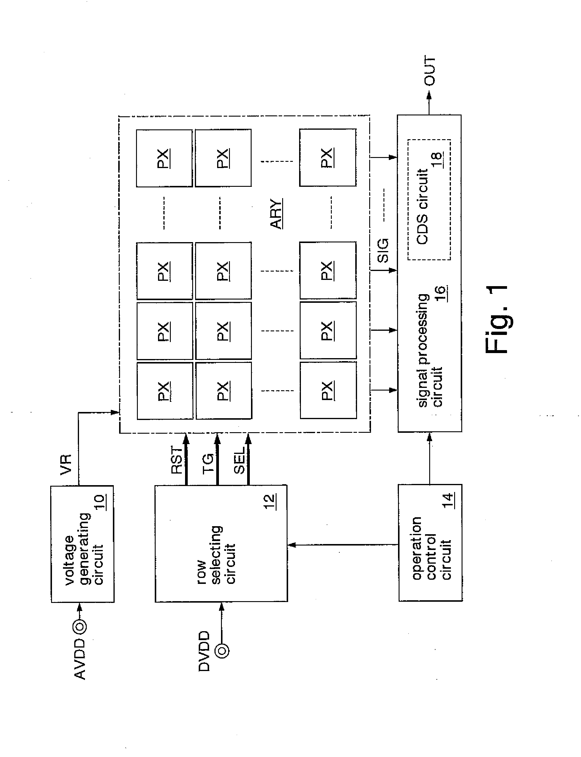
[0044]FIG. 1 shows an imaging device of the present invention. This imaging device is formed as an active pixel sensor chip on a silicon substrate, using a CMOS process. The imaging device includes a voltage generating circuit 10, a row selecting circuit 12, an operation control circuit 14, a signal processing circuit 16, and a pixel array ARY.

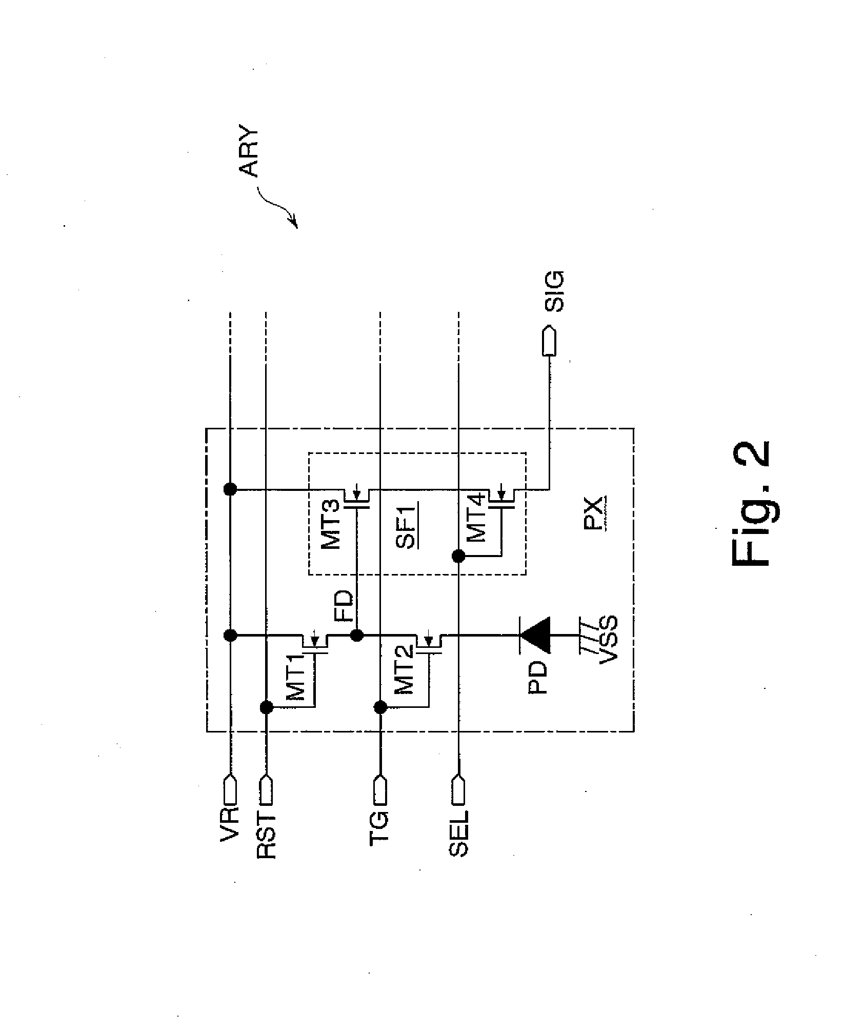
[0045] The voltage generating circuit 10 generates an internal voltage VR which is an always constant voltage in response to a power supply voltage AVDD. Incidentally, the voltage generating circuit 10 may modulate the internal voltage VR as necessary instead of generating the constant internal voltage VR. The power supply voltage AVDD is a power supply voltage for an analog circuit. The internal voltage VR is a voltage lower than the power supply voltage AVDD and always held at a constant voltage regardless of changes in the power supply voltage AVDD and changes in temperature. The row selecting circuit 12 outputs a reset signal RST, a transf...

fifth embodiment

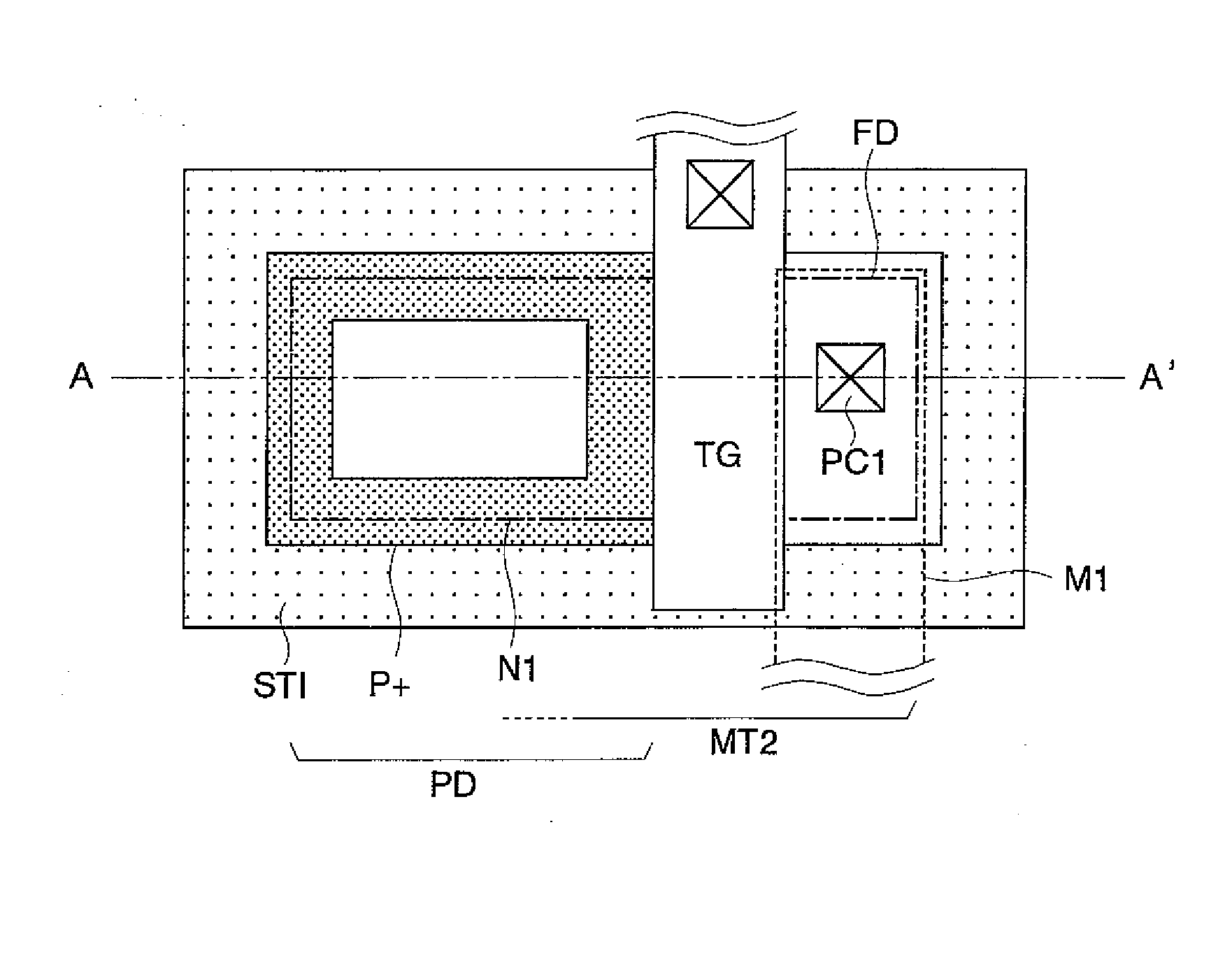
[0083] In the above fifth embodiment, the example in which the diffusion regions N2, N3 are formed in the inner part of the diffusion region N1 and the diffusion region N4 is formed at the surface of the diffusion region N1 is described. The present invention is not limited to this embodiment. For example, all the diffusion regions N2, N3, N4 may be formed at the surface of the diffusion region N1.


PUM


Abstract

First diffusion region constituting a photodiode in each pixel stores carriers generated according to incident light. Second diffusion region is formed at a surface of the first diffusion region to cover a peripheral part of the first diffusion region. In the peripheral part of the first diffusion region, crystal defects tend to occur by a process of forming an isolation region and a gate electrode, so that dark current noise tends to occur. The second diffusion region functioning as a protection layer prevents crystal defects in a manufacturing process. The second diffusion region isn't formed on a center of the surface of the first diffusion region where crystal defects don't tend to occur. In the first diffusion region where the second diffusion region isn't formed, the thickness of a depletion layer increases, which improves light detection sensitivity. This improves detection sensitivity of the photodiode without increasing the dark current noise.

Description

CROSS REFERENCE TO RELATED APPLICATION [0001] This application is a Continuation Application of International Application No. PCT / JP2005 / 005745, filed Mar. 28, 2005, and designating the U.S., the entire contents of which are incorporated herein by reference.BACKGROUND [0002] 1. Field [0003] The present invention relates to an imaging device including a photodiode. In particular, the present invention relates to a technique for improving detection sensitivity of the photodiode without increasing dark current noise. [0004] 2. Description of the Related Art [0005] An imaging device such as an active pixel sensor (hereinafter also referred to as an APS) has a plurality of pixels each including a photodiode. Light incident on the pixel is converted into optical carriers by the photodiode and outputted as an electrical signal to generate an image signal. Generally, the imaging device is formed using pixels called a three-transistor type and a four-transistor type (Japanese Unexamined Pate...

Claims


Application Information

Patent Timeline
Patent Type & Authority Applications(United States)
IPC IPC(8): H01L27/148H04N5/335H04N5/361
CPCH01L27/14603H01L27/14609H01L27/14621H01L27/14627H01L27/1463Y02E10/50H01L27/14645H01L31/03529H04N3/1568H04N5/335H04N5/361H01L27/14643H04N25/63H04N25/00
Inventor INOUE, TADAOYAMAMOTO, KATSUYOSHIKOBAYASHI
Owner SOCIONEXT INC
Why Eureka
Try Eureka